请问如图的电路该怎么分析?同向输入端和反向输入端之间怎么接了个大电阻?
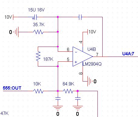
同向输入端的另一个输入可以看成一个电压源+内阻作为输入。
不好意思,前面表述的不清楚电路可简化成如下: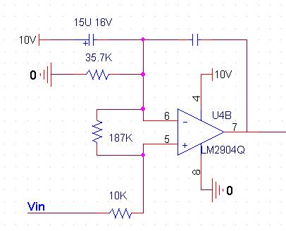
The big resistor between the two input terminal of OPamp is used to set the dc bias operation point, the two capacitor connected to the negative terminal of opamp set the small signal ratio of the whole circuit gain.
还是不大理解
再请教一下allen,我是这样想的如果考虑直流偏置,是不是说输入信号的直流分量会在放大器同反向输入端之间建立一个直流电压。
那么这个直流电压必须很小罗,否则放大器输出不是直接饱和了嘛?
Yes, you are right.
According to your schematic, the input common voltage is near the ground, and the output bias point need to be set by the dc input differnce voltage, otherwise, you can not get correct results,this is decied by the schematic's structure. Normally, this schematic is not good, if the input common voltage is bigger than zero, you need to bias the negative input terminal of opamp to your common input voltage.
哦,,,,,,,,看样子,这里还是卖E文的好地方.......
yes
分析得不错,的确是
基本同意
ding ding ding
进来参观学习一下啊。
学习了
dc bias