关于LM25118的AGND和PGND的区别
你好,我正在使用LM25118做一个电源方案,数据手册中关于AGND,PGND两个管脚的介绍很简单,在参考设计的管理图里是直接把两个角连一起的,评估板上却做了隔离,我想问一下,他们有什么区别,以及他们的具体作用,另外layout的时候要注意什么。
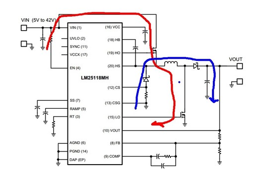
如图所示,红色路径与蓝色路径为此芯片的功率路径。因此都需要连接到PGND并且将两个环路尽可能的做到最小
其余管脚连接AGND最后AGND与PGND在焊盘上进行单点接地即可
关于PCB布板的具体细节详见datasheet26页
http://www.ti.com/lit/ds/symlink/lm25118-q1.pdf
PCB Layout and Thermal Considerations
In a buck-boost regulator, there are two loops where currents are switched very fast. The first loop starts from the
input capacitors, and then to the buck switch, the inductor, the boost switch then back to the input capacitor. The
second loop starts from the inductor, and then to the output diode, the output capacitor, the re-circulating diode,
and back to the inductor. Minimizing the PC board area of these two loops reduces the stray inductance and
minimizes noise and the possibility of erratic operation. A ground plane in the PC board is recommended as a
means to connect the input filter capacitors to the output filter capacitors and the PGND pins of the LM25118.
Connect all of the low current ground connections (CSS, RT, CRAMP) directly to the regulator AGND pin. Connect
the AGND and PGND pins together through topside copper area covering the entire underside of the device.
Place several vias in this underside copper area to the ground plane of the input capacitors