TPS767D301给F28335供电问题
用TPS767D301给28335供电,28335的datasheet上写是先上内核1.8V,后上I/O3.3V,那我需要给3.3V加个延时电路吗?
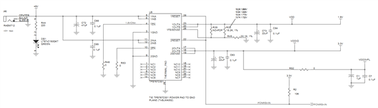
我看ezDSPf28335原理图中貌似没有给3.3V延时,两个EN端都直接接地了,是不是说这种同时上电的方式也可以?
还有掉电顺序是什么?要考虑吗?
Kevin Wong
用TPS767D301给28335供电,28335的datasheet上写是先上内核1.8V,后上I/O3.3V,那我需要给3.3V加个延时电路吗?
我看ezDSPf28335原理图中貌似没有给3.3V延时,两个EN端都直接接地了,是不是说这种同时上电的方式也可以?
还有掉电顺序是什么?要考虑吗?
请仔细阅读第127页。28355对上电时序没有特殊要求,只不过如果VDD比VDDIO后达到0.7V的话容易产生Glitch而已。
而TPS767D301的两路LDO,并没有Spec表明,自身有时序差别,所以可以认为是同时启动,产生Glitch的可能性极小。
但是如果你有单片机或者啥的去控制时序,最好不过了。
Power Sequencing
No requirements are placed on the power up/down sequence of the various power pins to ensure the
correct reset state for all the modules. However, if the 3.3-V transistors in the level shifting output buffers
of the I/O pins are powered prior to the 1.9-V transistors, it is possible for the output buffers to turn on,
causing a glitch to occur on the pin during power up. To avoid this behavior, power the V DD pins prior to or
simultaneously with the V DDIO pins, ensuring that the V DD pins have reached 0.7 V before the V DDIO pins
reach 0.7 V.
There are some requirements on the XRS pin:
1. During power up, the XRS pin must be held low for t w(RSL1) after the input clock is stable (see Table 6-
11). This is to enable the entire device to start from a known condition.
2. During power down, the XRS pin must be pulled low at least 8 μs prior to V DD reaching 1.5 V. This is to
enhance flash reliability.
No voltage larger than a diode drop (0.7 V) above V DDIO should be applied to any digital pin (for analog
pins, it is 0.7 V above V DDA ) prior to powering up the device. Furthermore, V DDIO and V DDA should always
be within 0.3 V of each other. Voltages applied to pins on an unpowered device can bias internal P-N
junctions in unintended ways and produce unpredictable results.
感谢您的帮助!