tpl0102程序问题
我把A2 A1 A0 连接在I/O口上,SDA,SCL连接在I2C上,程序如下,但是阻值无法进行控制。请问问题在哪里
//******************************************************************************
// MSP430G2xx3 Demo - USCI_B0 I2C Master Interface to TPL0102, Write
#include "msp430g2553.h"
void main(void)
{
WDTCTL = WDTPW + WDTHOLD; // Stop Watchdog Timer
P2DIR |= BIT7 + BIT6 + BIT5;
P2OUT &= ~0XE0; //Make A0 A1 A2 low power,p2.5~p2.7
P1SEL |= BIT6 + BIT7; // Assign I2C pins to USCI_B0
P1SEL2|= BIT6 + BIT7; // Assign I2C pins to USCI_B0
UCB0CTL1 |= UCSWRST; // Enable SW reset
UCB0CTL0 = UCMST + UCMODE_3 + UCSYNC; // I2C Master, synchronous mode
UCB0CTL1 = UCSSEL_2 + UCSWRST; // Use SMCLK, keep SW reset
UCB0BR0 = 12; // fSCL = SMCLK/12 = ~100kHz
UCB0BR1 = 0;
UCB0I2CSA = 0xA0; // Set slave address
UCB0CTL1 &= ~UCSWRST; // Clear SW reset, resume operation
IE2 |= UCB0TXIE; // Enable TX ready interrupt
UCB0CTL1 |= UCTR + UCTXSTT; // I2C TX, start condition
UCB0TXBUF = 0x00; // Write DAC control byte
__bis_SR_register(CPUOFF + GIE); // Enter LPM0 w/ interrupts
}
// USCI_B0 Data ISR
#pragma vector = USCIAB0TX_VECTOR
__interrupt void USCIAB0TX_ISR(void)
{
UCB0TXBUF = 0X10; // Transmit data byte
}
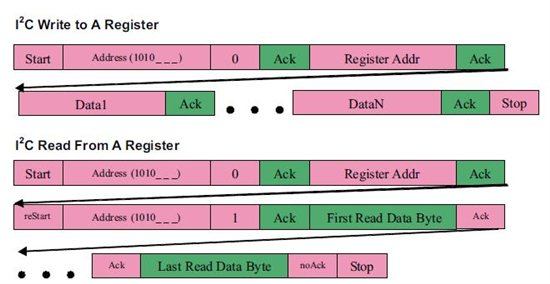
TPL0102是一个I2C的数字电位器.请确认下面管脚连接,以及你的时序与手册13~14页是否对应.
Potentiometer Pin Description
HA,HB,LA,LB
The high (HA, HB) and low (LA, LB) terminals of the TPL0102 are equivalent to the fixed terminals of a
mechanical potentiometer. The H and L terminals do not have any polarity restrictions, i.e. H can be at a higher
voltage than L, or L can be at a higher voltage than H. The WA and WB terminals are the wipers and equivalent
to the movable terminal of a mechanical potentiometer. The position of the wiper is set using the WR register.
With the WR register set to 255 decimal, the wiper is closest to the H terminal, and with the WR register set to 0,
the wiper is closest to the L terminal.
SDA, SCL
SDA is a bi-directional serial data input/output pin for I2C communication. SDA is an open drain output and
requires an external pull-up resistor.
SCL is the serial clock input for I2C communication. SCL requires an external pull-up resistor.
A0, A1, A2
These inputs are used to set the last three bits of the I2C address of the device. By using different values for A0,
A1, A2, up to eight TPL0102 devices can be used on the same I2C bus.
管脚连接应该没有问题,检查了好几遍,SDA,SCL连接的就是lauchpad上的I2C,现在调试结果是,数据感觉上是能写进去的,因为能进入中断,我觉得数据是在发送的,但是发送结束后,tpl0102的阻值都没有发生变化,有什么原因,或者我应该再从什么方面找。我的管脚连接是跟原理图画的是一样的,而且连接也是对的,我用万用表测了
老师,有没有什么差不多的示例代码可以参考吗?谢谢
首先需要确认的是时序,是否用示波器抓来看过?现成的代码没有,建议把时序发来看下:
另外这个I2C寄存器应该是可读的,有没有读回来看是否写对了?
请问SDA和SCL的上拉电阻值对数据的传输有影响吗,我这里用的是5.1K
代码如下
//******************************************************************************
// MSP430G2xx3 Demo - USCI_B0 I2C Master Interface to DAC8571, Write
//
// Description: Using UCB0TXIE, a continuous sine wave is output to the
// external DAC using a 16-point look-up table. Only one start condition
// is executed. Data is handled by the ISR and the CPU is normally in LPM0.
// ACLK = n/a, MCLK = SMCLK = BRCLK = default DCO = ~1.2MHz
//
// MSP430G2xx3 DAC8571
// ------------------ ------------
// -|XIN P1.7/UCB0SDA|<--------------->|SDA |
// | P1.6/UCB0SCL|---------------->|SCL I2C |
// -|XOUT | | SLAVE |
// | I2C MASTER | GND|A0 |
//
//
// DAC8571 I2C address = 0x4C (A0 = GND)
//
// D. Dang
// Texas Instruments Inc.
// February 2011
// Built with CCS Version 4.2.0 and IAR Embedded Workbench Version: 5.10
//******************************************************************************
#include "msp430g2553.h"
unsigned char a = 0;
unsigned char temp_tx = 0;
void main(void)
{
WDTCTL = WDTPW + WDTHOLD; // Stop Watchdog Timer
P2DIR |= BIT7 + BIT6 + BIT5;
P2OUT &= ~0XE0;
P1SEL |= BIT6 + BIT7; // Assign I2C pins to USCI_B0
P1SEL2|= BIT6 + BIT7; // Assign I2C pins to USCI_B0
UCB0CTL1 |= UCSWRST; // Enable SW reset
UCB0CTL0 = UCMST + UCMODE_3 + UCSYNC; // I2C Master, synchronous mode
UCB0CTL1 |= UCSSEL_2 ; // Use SMCLK, keep SW reset
UCB0BR0 = 12; // fSCL = SMCLK/12 = ~100kHz
UCB0BR1 = 0;
UCB0I2CSA = 0xA0; // Set slave address
UCB0CTL1 &= ~UCSWRST; // Clear SW reset, resume operation
IE2 |= UCB0TXIE; // Enable TX ready interrupt
UCB0CTL1 |= UCTR + UCTXSTT; // I2C TX, start condition
_EINT(); // w/ interrupts
for(;;)
{
while (UCB0CTL1 & UCTXSTT); // Loop until I2C STT is sent
UCB0CTL1 |= UCTR + UCTXSTT; // I2C TX, start condition
}
}
//USCI_B0 Data ISR
#pragma vector = USCIAB0TX_VECTOR
__interrupt void USCIAB0TX_ISR(void)
{
temp_tx++;
if(temp_tx==1)
{
UCB0TXBUF = 0X01; // Transmit data byte
a = UCB0RXBUF;
}
else if(temp_tx>=2)
{
UCB0TXBUF = 0XFF;
}
else if(temp_tx == 200)
{
temp_tx = 1;
}
}
我检测了一下SCL,SDA,波形如图所示,另外,我尝试读取I2C的寄存器,好像没成功,您帮我看看吧,谢谢啦!一次好像只能放一个图,另一个在下面
另一张图,麻烦你了
硬件工程师要用两个探头同时抓data和clock看是否满足时序关系,然后你自己仔细数下你发的数值和软件给的是否一致,然后读取的时候看有没有响应。单独抓两张图是看不出来关系的:
读取没有成功说明I2C通信没有成功的,仔细看发的数是否正确时序是否满足手册要求吧,
老师好,现在我两个一起看了一下,单片机一直在重复发,start 和slave address两个信号110100000110100000.。。。一直接受不到ack信号,不知道该怎么办了,
同学I2C其实比较简单,如果不通的话一般两种可能:时序不满足要求或没有焊好.排除焊接问题后请仔细检查是否满足手册要求,仔细读手册12~15页
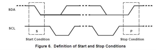
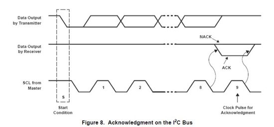
I2C communication with this device is initiated by the master sending a start condition, a high-to-low transition on
the SDA input/output while the SCL input is high (see Figure 6). After the start condition, the device address byte
is sent, MSB first, including the data direction bit (R/W). This device does not respond to the general call
address. After receiving the valid address byte, this device responds with an ACK, a low on the SDA input/output
during the high of the ACK-related clock pulse.
也就是说在你的时序图中只有起始位和7位地址8个脉冲,没有响应位,换句话说,I2C总线上根本没有数据传输,I2C的时序不正确,可检查下芯片焊接,上拉电阻阻值,如果挂有多个从机,看从机地址是否准确,或者参考下其他成功的I2C的例子。
现在我两块lauchpad之间的通信是没有问题的,但是连接到tpl0102时就没反应的,不知道是什么原因。。
I2C 总线上一共挂了3个从机?建议将其他从机去掉,直接查看430和TPL0102是否通信异常
不是的,我先试了430之间的通信,然后是可以的,然后再去试tpl0102的,没有都连在一起的。都是单独分开试的。有一个很奇怪的地方,两个单片机之间通信的时候UCB0CTL1上的UCTXSTT是可以被置1的,但是和tpl0102练的时候就是置不了1.很是费解
问题已经解决了,主要是slave address 写错了。 改正过来之后就对了。。
感谢所有大神的帮助!
您好,我现在初学430,现在用TPL0102,然后我遇到了和您一样的问题,我已经看了好多天了,还是没有效果。能否给小弟一个例程研究一下呀。。。
能给个tpl0102例程否?
有没有模拟IIC操作电位器的程序啊