CC1310 ADC参考源问题
您好:
目前想要使用CC1310的ADC,当时对于参考源不是很明白
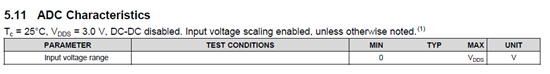
The ADC supports two different internal references, one constant and one relative to VDDS.
The ADC automatically scales down the input signal to be within the reference range. It is possible to
disable the scaling, but this requires great care by the user to ensure the maximum ratings in the data
sheet are followed. With scaling enabled, the internal fixed reference looks like 4.3 V compared to the
actual input level. With scaling disabled, the reference is 1.44 V.
手册上是这样写的,可使用内部的固定参考源或者与VDDS有关的参考源。
1.44V的可以理解,需要人为控制输入电压避免超过限制;
但是开启了Scaling后,加粗的部分不能理解是什么意思,是说我的待测量电压如果超过4.3V就会被自动个降压吗。但是芯片电源只有3V或者2V,怎么会出来4.3V的电压呢,是内部的升压吗。开启了Scaling之后的ADC应该如何理解呢?
谢谢!
就是等效的,实际不可能有这个电压的。
就是说,从计算上“看上去”是个4.3V的参考源。
那您看是不是,如果我用2V电压做CC1310电源,从AD输入一个3.5V的电压的话,程序也能够检测出来呢?
谢谢!
首先要保证输入电压要低于Datasheet允许的最大电气规格的要求
内部4.3V是等效出来的。
根据scaling是否打开,基准分别为1.44V 和4.3V