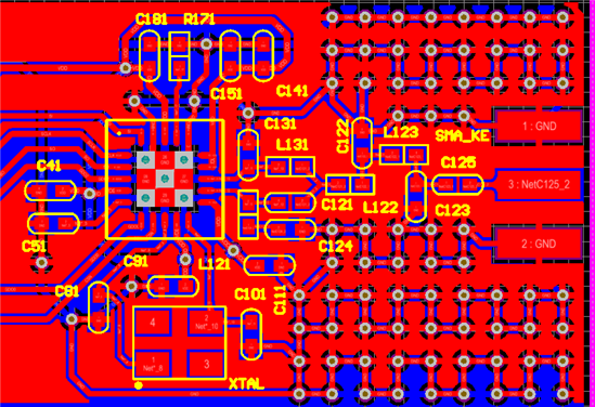
自己画的CC1101PCB还存在哪些问题?请指教?
自己做毕设需要用到CC1101的无线功能,通过买现成的模块已经实现了基本功能,接着自己按照TI官方的参考设计制作了CC1101无线模块,外围器件参数也是按照官方手册给的,调试按照SmartRF配置的寄存器,但是通信距离没有买的现成模块好用,所以想传上自己的PCB图,希望大家能帮我看看我PCB不合理的地方?谢谢啦!然后我还有下面几个问题?
1.CC1101芯片下方裸露焊盘需要和PCB上相应的接地部分焊接在一起吗?还是只要接触就好了?
2.晶振负载电容用22pf或者是27pf都在允许范围呢吗?还是说哪个更好一些?
下面是我的PCB图

先对照下面的checklist来看看是否满足下面的要求
The checklist below provides important RF PCB design considerations to be followed, and it
is highly recommended that the designers verify their designs with the suggested points
below. Following these points in the checklist will help to achieve optimum performance from
the designs.
1 Ensure that you follow the datasheet layout recommendation unique to the part
(CCXXXX).
2 0603(mils) discrete parts are not recommended because of size and parasitic
values.
3 Verify that bypassing capacitors are as close as possible to the power supply pins
that they are meant to bypass.
4 Ensure each decoupling capacitor only decouples the specific pins recommended
on the reference design and that the capacitor is correct value and type.
5 Ensure that decoupling is done pin<>capacitor<>via.
6 Verify the stack-up matches the reference design. If the design is a 4-layer PCB;
verify that ground plane is layer two right below top/component side.
7 Changing the layer spacing/stack-up will affect the matching in the RF signal path
and should be carefully accounted for as explained in AN068 [2].
8 Verify that the ground plane matches the reference design. There should be a
solid ground plane below the device and the RF path. There should be no ground
plane below the antenna unless you are using an antenna whose manufacturer
recommends a ground plane (for example, a whip antenna).
9 Verify that RF signal path matches the reference design as closely as possible.
Components should be arranged in a very similar way and oriented the same way
as the reference design.
10 The crystal oscillator should be as close as possible to the oscillator pins of the
part. Long lines to the oscillator should be avoided if possible.
11 Verify that the top ground pours are stitched to the ground plane layer and bottom
layer with many vias around the RF signal path. Compare to the reference design.
Vias on the rest of the board should be no more than λ/10 apart.
12 If the part has a differential output, ensure that the traces in the differential section
are symmetrical as in the reference design.
13 If the design uses a battery (such as a coin cell), the battery will act as a ground
plane and should therefore not be placed under the antenna.
14 If the reference design specifies using T-Lines (Transmission Lines), it is very
critical to ensure that the T-Lines match the reference design exactly.
15 Verify that the under-the-device power pad layout is correct. The solder pads and
mask should match and the opening size should ensure correct amount of paste.
Vias should be the correct number and masked/tented to ensure that they don’t
suck up all the solder, leaving none to solder the chip to pad. (Refer to the
datasheet for layout recommendation for the corresponding part.)
16 The board should specify impedance controlled traces. That is, the layer spacing
and FR4 permittivity should be controlled and known.
Important considerations for Antennas:
17 If using an antenna from a TI reference design, be sure to copy the design exactly
and check if the stack-up in the reference design matches your stack-up.
18 Changes to feed line length of antenna will change input impedance match.
19 Any metal in close proximity, plastic enclosure, and human body will change the
antenna’s input impedance and resonance frequency, which must be considered in
the design.
20 For multiple antenna on same board, use antenna polarization and directivity to
isolate.
21 For chip antennas verify that the spacing from and orientation with respect to the
ground plane is correct as specified in antenna’s datasheet.
22 It is a good practice to add a pi-network after the balun filter network for antenna
impedance matching. Component values can be calculated after the PCB is
fabricated and impedance measurement looking into antenna and the balun
network as made at the desired frequency. If not required, the shunt components
can be left un-mounted and a 0 ohm resistor can be used as series component.
你参考的具体是哪个设计?板子的层叠结构是怎样的?
谢谢你啊!我刚刚仔细看了你上面的一些要求。
1.我参考的设计是TI官方的433Mhz的设计,器件参数也是和官方推荐的一样的,使用村田系列的,但在晶振的负载电容上有点区别,我的负载电容是按照CC1101芯片datasheet给的两个27pf,但在TI给的CC1101_433Mhz的原理图中负载电容分别是12pf和15pf。负载电容是不是要按照具体的26M晶振推荐的负载电容来设置啊?
2.我做的是2层板,射频信号输出部分的balun等和官方参考设计基本一致,晶振部分布局有点远了啊,这个不好,我下次会改正。
3.然后关于地我不太懂啊,上面说天线下方应该没有地平面,是指天线下面的板子两层都不铺地吗?但是我看参考设计里面天线座下面铺地了啊。
4.还有PCB板材,我当时没给厂家说,按照普通的板子做的。后来我也了解到板材会有影响,这个FR-4板材该给厂家指定为高频板用的板材吗?
我的问题有点多啊,不好意思,我自己不是学无线通信专业,对这方面真的不太懂,刚好毕设要用一下无线模块,结果我自己做的板子效果不好,想在提升一下。麻烦了!
yifan xu
1.我参考的设计是TI官方
1.我参考的设计是TI官方的433Mhz的设计,器件参数也是和官方推荐的一样的,使用村田系列的,但在晶振的负载电容上有点区别??我的负载电容是按照CC1101芯片datasheet给的两个27pf,但在TI给的CC1101_433Mhz的原理图中负载电容分别是12pf和15pf。负载电容是不是要按照具体的26M晶振推荐的负载电容来设置啊?
最好按照参考设计的bom,如果不行,是需要调的。就是打一个CW波,然后调整负载电容即可。
2.我做的是2层板,射频信号输出部分的balun等和官方参考设计基本一致,晶振部分布局有点远了啊,这个不好,我下次会改正。
okay
3.然后关于地我不太懂啊,上面说天线下方应该没有地平面,是指天线下面的板子两层都不铺地吗?但是我看参考设计里面天线座下面铺地了啊。
你这个是“连接器”不是天线。天线是要做地的净空的。
4.还有PCB板材,我当时没给厂家说,按照普通的板子做的。后来我也了解到板材会有影响,这个FR-4板材该给厂家指定为高频板用的板材吗?
FR4支持这个频段没问题的。就是你要和板厂说射频线要做阻抗控制。
有一些guideline可以看一下我的视频:
http://edu.21ic.com/lesson/1637
谢谢你啊!我仔细看了你的视频,收获很大,对于下一版的布局有些信心了,可我还有一个地方不太清楚,射频线的阻抗控制具体指那些射频线啊!

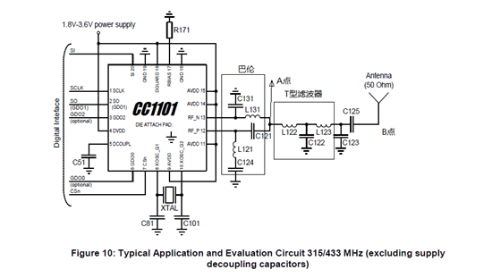
这是TI给的原理图,巴伦电路讲平衡信号转化为非平衡信号,T型滤波器虑去高次谐波,阻抗匹配电路是从RF-N和RF-P两个端口之间到天线之间之间整个电路吗?那射频线的阻抗控制意思从RF-N和RF-P出来到天线接口的所有的PCB上走线都要控制为50Ohm吗?还是只有C125出来到天线的那根射频线需要控制为50Ohm啊?
谢谢你啊!我仔细看了你的视频,收获很大,对于下一版的布局有些信心了,可我还有一个地方不太清楚,射频线的阻抗控制具体指那些射频线啊!

这是TI给的原理图,巴伦电路讲平衡信号转化为非平衡信号,T型滤波器虑去高次谐波,阻抗匹配电路是从RF-N和RF-P两个端口之间到天线之间之间整个电路吗?那射频线的阻抗控制意思从RF-N和RF-P出来到天线接口的所有的PCB上走线都要控制为50Ohm吗?还是只有C125出来到天线的那根射频线需要控制为50Ohm啊?
嗯,都按照50ohm控制就好了。
就像视频里说的,巴伦部分的电长度很重要,所以这些部分的长度也要完全copy就对了。
