CC1310F128RSM
CC1310F128RSM 请问哪里有 这个芯片的引脚图, 官网上只有简单 介绍,一些端口复用,没有具体标明,
49脚 7mm*7mm 的串口位置IO2与IO3 在 32 脚 4mm*4mm 中IO3位置是JTAG_TDO, 我想问这有影响吗
你要看reference manual,看如下手册的11.8 I/O Pin Mapping [pg988]
http://www.ti.com/lit/pdf/swcu117
11.3 I/O Mapping and Configuration
The MCU IOC can map a number of peripheral modules such as GPIO, SSI (SPI), UART, I2C, and I2S to
any of the available I/Os. The peripherals AUX and JTAG are limited to specific I/O pins. Each type of
peripheral signal has a unique PORTID that can be assigned to selected I/O pins (referenced as DIOs).
Table 11-3 lists the different PORTID signals.
11.3.1 Basic I/O Mapping
To map a peripheral function to DIOn, where n can range from 0 to a maximum of 31, the PORTID and
pin configuration must be set in the corresponding IOC:IOCFGn register. To select what kind of function
the pin must be routed, choose the PORTID number for the desired peripheral function and write the
PORTID number to the IOC:IOCFGn.PORTID bit field.
The function can be set by using the following driver library function:
IOCPortConfigureSet(DIOn, PORTID, PIN-CONFIG);
See Section 11.6 to see the kind of configurations that can be set in PIN-CONFIG.
11.3.2 MAP AUXIO From the Sensor Controller to DIO Pin
There are up to 16 signals (AUXIO0 to AUXIO15) in the sensor controller domain (AUX). These signals
can be routed to specific pins given in Table 11-2. AUXIO0 to AUXIO7 have analog capability, but can
also be used as digital I/Os, while AUXIO8 to AUXIO15 are digital only. The signals routed from the
sensor controller domain (AUX) are configured differently than GPIO and other peripheral functions. This
section does not cover the use of all the capabilities of the sensor controller (for more details, see
Chapter 17).
In this example, AUXIO1 is mapped to DIO29 on the 7 × 7 package type and set up as a digital input. The
pin number and DIO number differs for different package types. The module must be powered, and the
clock to the specific module within the AUX domain must be enabled (AIODIO1 for AUXIO0 to AUXIO7).
4x4 和7x7 引脚安排本来就是不一样的,如下图:
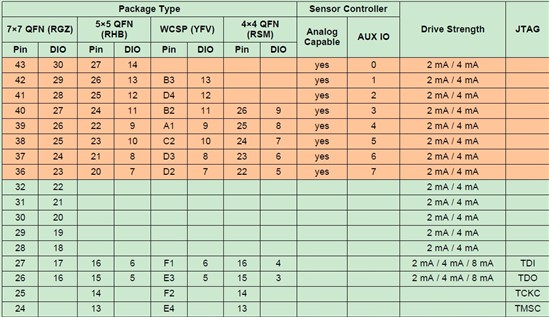
如果你是7X7就按7X7的引脚来画原理图,JTAG,电源供电要特定管脚,功能管脚是可以软件定义的