17W双输出反激转换器-LNK6774V参考设计
led circuit diagram, the entire bill of materials required to build the supply, extensive documentation of the power transformer, along with test data and waveform plots of the most important electrical waveforms. This report describes a universal input, 5 V, 1000 mA and 18 V, 670 mA isolated flyback converter employing LNK6774V from the LinkSwitch-HP family of ICs. It contains the complete specification of the power supply, a detailed circuit diagram, the entire bill of materials required to build the supply, extensive documentation of the power transformer, along with test data and waveform plots of the most important electrical waveforms. This report describes a universal input, 5 V, 1000 mA and 18 V, 670 mA isolated flyback converter employing LNK6774V from the LinkSwitch-HP family of ICs. It contains the complete specification of the power supply, a detailed circuit diagram, the entire bill of materials required to build the supply, extensive documentation of the power transformer, along with test data and waveform plots of the most important electrical waveforms.
17W双输出反激转换器参考设计主要特性和指标:
? Primary side regulated isolated flyback converter with ±5% regulation.
? 132 kHz switching frequency for small transformer and output filter size
? Full load continuous conduction mode operation for improved efficiency and reduced output capacitor ripple currents
? Multi-mode operation maximizes efficiency over full load range
? Below 100 mW power consumption with 50 mW standby load at 230 VAC.
? Extensive protection features including OVP, OTP, brown-in/out, line overvoltage, and lost-regulation (auto-restart)
? Meets EN-550022 and CISPR-22 Class B conducted EMI with 5 dB margin.
? Meets IEC61000-4-5 1 kV / 2 kV surge.
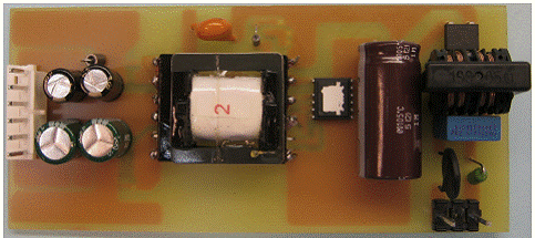
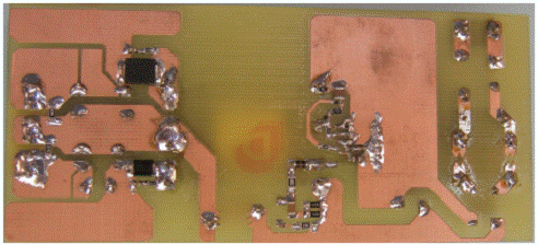
图3. 17W转换器参考设计外形图
17W转换器参考设计主要性能指标:
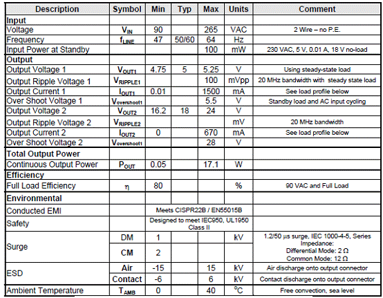
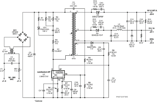
图4. 17W转换器参考设计电路图
17W转换器参考设计材料清单:
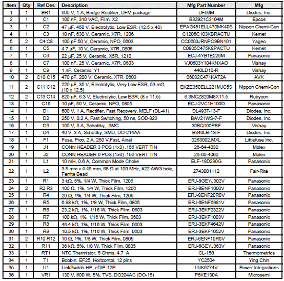
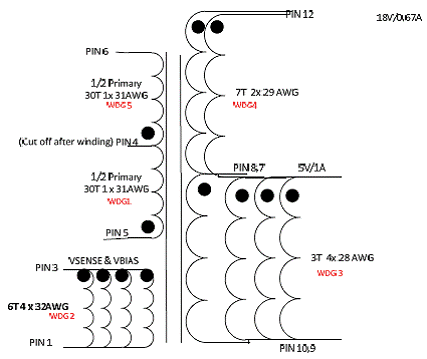
图5. 17W转换器参考设计变成压器电路图
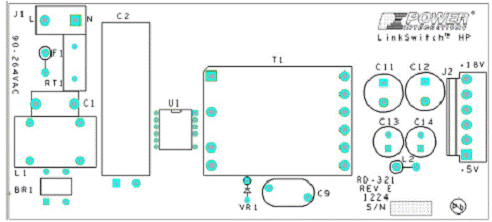
图6. 17W转换器参考设计PCB布局图
- 离线型LED驱动器GreenPoint参考设计(11-29)
- 智能线性LED驱动器LM3466参考设计(03-07)