AD9644:14位串行模数转换器应用详解(原创)
s limit the input bandwidth. Refer to the AN-742 Application Note, Frequency Domain Response of Switched-Capacitor ADCs; the AN-827 Application Note, A Resonant Approach to Interfacing Amplifiers to Switched-Capacitor ADCs; and the Analog Dialog article, "Transformer-Coupled Front-End for Wideband A/D Converters," for more information on this subject (refer to www.analog.com).
For best dynamic performance, the source impedances driving VIN+ and VIN− should be matched, and the inputs should be differentially balanced.
输入模式
The analog inputs of the AD9644 are not internally dc biased. In ac-coupled applications, the user must provide this bias externally. Setting the device so that VCM = 0.5 × AVDD (or 0.9 V) is recommended for optimum performance. An on-board common-mode voltage reference is included in the design and is available from the VCMA and VCMB pins. Using the VCMA and VCMB outputs to set the input common mode is recommended. Optimum performance is achieved when the common-mode voltage of the analog input is set by the VCMA and VCMB pin voltages (typically 0.5 × AVDD). The VCMA and VCMB pins must be decoupled to ground by a 0.1 μF capacitor. This decoupling capacitor should be placed close to the pin to minimize the series resistance and inductance between the part and this capacitor.
差分输入配置
Optimum performance is achieved while driving the AD9644 in a differential input configuration. For baseband applications, the AD8138, ADA4937-2, and ADA4938-2 differential drivers provide excellent performance and a flexible interface to the ADC.
The output common-mode voltage of the ADA4938-2 is easily set with the VCM pin of the AD9644 (see Figure 2), and the driver can be configured in a Sallen-Key filter topology to provide band limiting of the input signal.
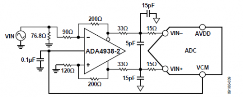
Figure 2. Differential Input Configuration Using the ADA4938-2
For baseband applications in which SNR is a key parameter, differential transformer coupling is the recommended input configuration. An example is shown in Figure 3. To bias the analog input, the VCM voltage can be connected to the center tap of the secondary winding of the transformer.
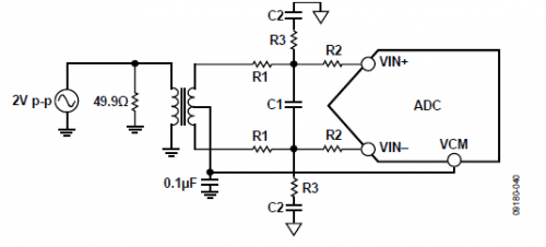
Figure 3. Differential Transformer-Coupled Configuration
The signal characteristics must be considered when selecting a transformer. Most RF transformers saturate at frequencies below a few megahertz (MHz). Excessive signal power can also cause core saturation, which leads to distortion.
At input frequencies in the second Nyquist zone and above, the noise performance of most amplifiers is not adequate to achieve the true SNR performance of the AD9644. For applications in which SNR is a key parameter, differential double balun coupling is the recommended input configuration (see Figure 4). In this configuration, the input is ac-coupled and the VCM is provided to each input through a 33 Ω resistor. These resistors compensate for losses in the input baluns to provide a 50 Ω impedance to the driver.
In the double balun and transformer configurations, the value of the input capacitors and resistors is dependent on the input fre-quency and source impedance. Based on these parameters the value of the input resistors and capacitors may need to be adjusted or some components may need to be removed. Table 9 displays recommended values to set the RC network for different input frequency ranges. However, these values are dependent on the input signal and bandwidth and should be used only as a starting guide. Note that the value
AD9644 相关文章:
- AD9644:14位串行模数转换器概述(08-09)