为电网注入绿色能源
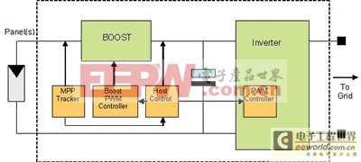
required ac output current. For this, the inverter monitors the grid voltage and frequency, and its own output current, to appropriately control the inverter stage.
The inverter really works as an ac current source, driving the grid impedance. The intermediate voltage has to be higher than the desired peak output voltage, plus some margin – at 220 Vrms, the peak voltage is 308 V, so the intermediate dc bus voltage is usually chosen to be 350 to 390 V. This means the second inverter can act as a pure step-down circuit, simplifying the topology.
It is not uncommon to find several boost converters connected in parallel, to be able to connect multiple strings of panels. They all feed into one inverter.

Fig. 2. The maximum power point tracker helps the inverter draw the maximum power for the inverter to convert to ac output current.
Figure 3 shows an inverter, with the main PCB dedicated to the power conversion. In the center, power IGBTs can be seen under clips that press them to a heat sink. On the right, electrolytic caps are used as intermediate caps between the boost converter and the inverter, to store the energy needed to bridge individual 50 Hz cycles. This is a transformer-less inverter, and the two big inductors on the top are the output inductors.

Fig. 3. Small inverter for 3kWp output power.
Depending on safety requirements and, to some extent, the panel types and installation, a PV inverter may be required that provides isolation. This can be done with a transformer, where the inverter from above block diagram will drive the transformer with a high frequency, and then a second stage with rectification and dc to ac conversion is required to produce 50 or 60 Hz ac for feeding the grid. Unfortunately, this means the efficiency drops by 1% to 2%.
Topology choice
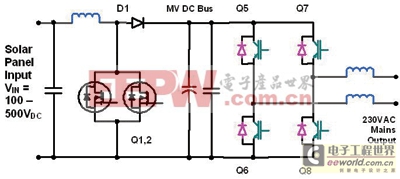
Figure 4 shows the classical topology of a boost converter, followed by a H-bridge. The transistors Q1 and Q2 are parallel, which is not uncommon in this stage and done simply to achieve lowest conduction losses.

Fig. 4. Typical boost converter followed by H-converter bridge.
This stage is followed by a capacitor, to stabilize the voltage that goes into the H-bridge and provide a certain holdup time. This capacitor will have to be an electrolytic capacitor in many cases, due to the size required, and this is probably the most important factor determining system reliability the inverter will see around 7,000 temperature cycles in a 20-year lifetime, and this is a huge strain for electrolytic caps.
In the inverter or dc-to-ac section of the system, some of the devices can be switched at line frequency whereas others are switched with the conversion frequency. If done cleverly, the first devices can be chosen for lowest conduction losses, like the non-punch-through (NPT) Fieldstop (FS) IGBTs from Fairchild Semiconductor, whereas the latter should be chosen for lowest switching losses.
Here, a combination of different IGBTs or even IGBTs and MOSFETs can help to improve the overall yield. And to properly drive the power switches, optically isolated gate drivers like Fairchild’s FOD3180 can be used, improving the system reliability where high dv/dt can suddenly occur, such as in the case of a grid fault.
The topology choice also implies a certain method to adapt the output behavior to the grid load. Here, new regulations are being implemented, forcing the inverters to contribute more to the local grid quality than before.
In certain areas, where many PV systems are connected, the phase lead of the output current of the inverters can lead to local breakdowns, simply
- 四种思路 四大光伏逆变器并网方式(12-09)
- 光伏逆变器转换效率两大决定因素(12-09)
- 两大主要因素决定光伏逆变器的转换效率(12-08)
- 光伏逆变器特有c知多少?(12-07)
- 光伏逆变器MPPT效率的计算方法与来源(12-07)
- 抑制漏电流:新型单相双Buck光伏逆变器方案(12-31)
