How to build a simple, interactive digital vol
The operation of the code
After reset, the microcontroller displays the photocell voltage on channel six. The more light the cell receives, the lower the voltage is across it. Effectively, the voltage at the ADC pin is directly related to the amount of light present. This is because the photocell is part of the voltage-divider on AN6 (see Figure 4). In fluorescent lighting, the voltage will sit around 2V. If you shade the corner of the board that contains the cell, the voltage will drop a bit; completely covering the photocell with your finger will drop the voltage to approximately 0.5V. Removing your finger will return the voltage to 2V.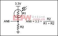
Figure 4. The voltage-divider and the equation that determines the voltage.
Note: you may notice that without any input connected to one of the AN pins, the voltage displayed is close to 1.4V. This results from internal bias circuitry and does not affect measurement.
The MAXQ2010 features an internal LCD driver which has two registers to control its operation. The values written to them set up the default mode for this board. LCRA = 0x1860; /* 1/4 duty, 32kHz clock, ground VADJ internally */LCFG = 0x7F; /* Activate segments on P0-P3, enable LCD, normal mode */
In this default mode, the segments are set up as shown in Figure 5.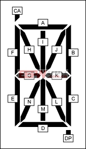
Figure 5. LCD display configuration.
A character is written by sending the high byte of the hex code (CAfedabcDP) to an LCD register, and the low byte (ijklhgnm) to the consecutive LCD register. This application includes a constant character table that can be used to look up the hex codes for the decimal digits. The character table makes displaying digits on the LCD very easy.
The 5-way switch (SW1) uses port pins P4.0 through P4.5. The common pin of SW1 is P4.0 which is set to output low. The other pins are connected to weak pullups by setting the direction to input and writing a 1 to the output. Thus, if a pin has a logic 0 on it when it is sampled, the program knows that the switch is pressed. After each ADC sample, the microcontroller polls the switch and changes the channel accordingly.
It is important to know that all the ADC configuration and data registers are accessed through the Conversion Sequence Address Register (ADDATA), and that the Status Register (ADST) points to the current register. Write instructions to ADDATA will write to the configuration registers and read instructions will read from the data registers.
The ADC is initialized by setting up the ADC Control Register (ADCN) and the configuration registers. First, we must load ADST with the configuration register to which we want to write first. After writing to ADDATA, ADST will automatically increase. Thus eight consecutive writes to ADDATA, when the initial register is Configuration Register 0, will write to registers 0 through 7. Each configuration register controls the configuration for that channel. Writing a 0x07 to the ADADDR instructs the microcontroller to start the conversion sequence with channel 0 and end with channel 7. This will cause the ADC to sample each channel once before raising a flag signaling that the data is ready.
Each result placed in a Data Register is accessed through ADDATA. To start at Data Register 0, ADST is set to 0. Eight reads from ADDATA retrieve all eight values of the conversion sequence. Here, the data register also increases with consecutive reads from ADDATA.
Each value read from ADDATA ranges from 0 to 4095. For the MAXQ2010, 4095 represents the ADC reference voltage, AVDD, which is typically 3.3V. The program scales the 12-bit value up to a range from 0 to 33000 instead of down to 3.3 because integer division would cause truncation. For example, an ADC value of 2036 would be displayed as 1.0000 instead of 1.6407. unsigned int voltage = ADCvalue * 3.3 * 10000 / 4095;
The result of this code is a value from 0 to 33000. The digits are masked off and displayed on the LCD with the decimal point added in the correct place. Essentially the conversion of the bit value is to 10-4 volts. Adding the decimal place later reverts the value back to volts.
interactive voltmeter digital simple ЯрЙиЮФеТЃК