Negative Charge Pumps Achieve
voltage than might otherwise be necessary. It is always best for the driver to stay in a high-efficiency mode as long as possible while the battery voltage falls. However, this performance requires minimum loss in the power switches and, consequently, more space and cost.
As noted above, the best conversion efficiency is offered by a 1x transfer mode, but this mode can only be used when the battery voltage is more than the WLEDs’ forward voltage (VF). The key to utilizing 1x mode for the lowest possible battery voltage has usually focused on lowering both the voltage drop of the 1x mode bypass FET and that of the current regulator. These voltage drops determine the series losses and minimum input voltage that can sustain 1x mode. The minimum battery voltage required by 1x mode is:
VIN(MIN_1X) = VLED + bypass pFET RDS(ON) × (ILED + VDROPOUT of the current regulator)
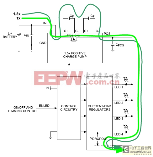
A traditional positive-charge-pump WLED solution uses a pFET bypass switch to connect the battery voltage to the WLEDs, as shown in Figure 1. This FET’s RDS(ON) is typically 1Ω to 2Ω. Further resistance reductions are limited since lower resistances typically would necessitate a larger FET, increasing the cost of the power device. 
Figure 1. In 1x mode, the positive charge pump uses an internal switch to bypass VIN to the WLEDs' anodes.
A positive charge pump generates 1.5x VIN or 2x VIN to drive the WLED anodes when VIN is insufficient to drive a 1x transfer mode. To implement the 1x mode in a positive-charge-pump architecture, we must use an additional internal switch to route VIN directly to the WLEDs’ anodes, thereby bypassing the charge pump.
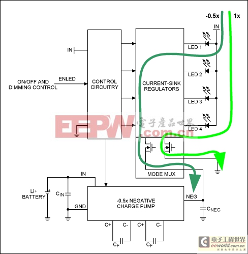
A negative-charge-pump architecture also generates -0.5x VIN to drive WLED cathodes when VIN is insufficient for the task. This architecture, however, does not require that you bypass the -0.5x VIN charge-pump output to ground in 1x mode because current regulators control the WLEDs’ current directly from VIN to ground. As a result, the negative-charge-pump architecture extends 1x mode all the way down t
VIN(MIN_1X) = VLED + VDROPOUT of the current regulator
Figure 2 shows the current path of 1x mode with a negative charge pump. The circuit does not require a pMOS bypass switch, and it directly regulates WLED current from VIN to ground. If ILED is 100mA total (i.e., 5 WLEDs × 20mA), a 2Ω pMOS bypass switch’s voltage drop would be 200mV. As it discharges, the Li+ battery voltage holds relatively stable around the 3.6V to 3.8V (typical) voltage range. Assuming a typical Li+ battery-discharge curve, the 200mV increase in operating voltage enabled by 1x mode dramatically improves efficiency.
Figure 2. Individual switchover for each WLED is possible when the driver switches to its negative-charge-pump mode, which improves overall efficiency
Maximizing Efficiency at Each LED Forward Voltage
In a traditional 1x/1.5x positive-charge-pump WLED driver, the WLED anodes connect to the charge pump’s output. If the WLEDs are mismatched, the driver must switch to 1.5x mode when there is not enough (VIN - VLED) headroom to support the worst forward-voltage WLED.
With the negative-charge-pump architecture, it is no longer necessary to abandon the efficient 1x mode due to the bad forward voltage of only one WLED. As Figure 2 illustrates, the Mode Mux circuit individually selects 1x mode or -0.5x mode for each WLED, thereby maximizing overall efficiency.
The charge-pump drivers, for example, turn on the -0.5x charge pump when the input voltage is insufficient to drive the highest forward-voltage WLED. In this situation, the devices drive only the highest VF WLED through the -0.5x negative rail (instead of ground), while the WLEDs with lower forward voltages remain in 1x mode.
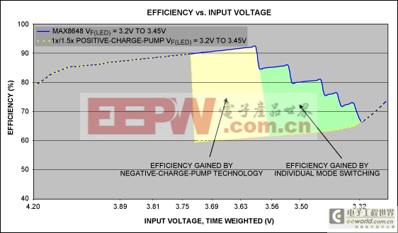
To further improve efficiency, the MAX8647/MAX8648 provide individual mode switching for the WLEDs. This technology adaptively switches the WLEDs to -0.5x mode at different times and at different VIN levels due to VF mismatches or temperature changes (Figure 3).
Figure 3. The efficiency of the MAX8647/MAX8648 charge-pump WLED drivers can be extended by switching to a negative-charge-pump mode and to individual mode switching for each WLED
模拟电路 模拟芯片 德州仪器 放大器 ADI 模拟电子 相关文章:
- 12位串行A/D转换器MAX187的应用(10-06)
- AGC中频放大器设计(下)(10-07)
- 低功耗、3V工作电压、精度0.05% 的A/D变换器(10-09)
- PIC16C5X单片机睡眠状态的键唤醒方法(11-16)
- 用简化方法对高可用性系统中的电源进行数字化管理(10-02)
- 利用GM6801实现智能快速充电器设计(11-20)
