升压转换器具有较高的轻负载效率-Boost Converte
时间:05-26
来源:互联网
点击:
In most DC-DC converters, the normal supply currents do not allow high efficiency at low load currents. The circuit in Figure 1, however, contains micropower components that enable it to maintain 90% efficiency for load currents as low as 1mA. IC1 (a quad Schmitt-trigger NAND gate) draws maximum quiescent currents of only 0.25μA, and IC2 (a combination voltage reference and comparator) draws only 2.5μA.
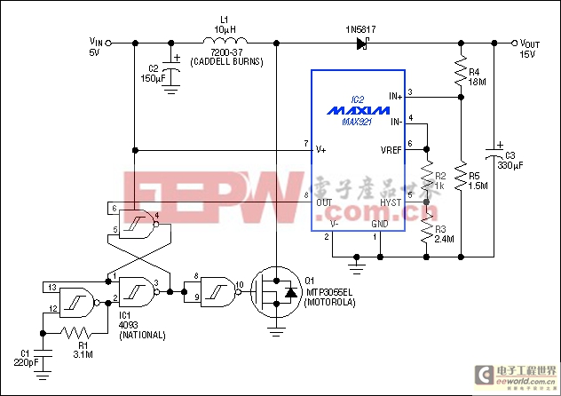
Figure 1. Consuming only microwatts of power, this 5V-to-15V boost converter provides low load currents with high efficiency.
IC2 compares its own reference voltage against the circuit output, VOUT. The resulting comparator output (pin 8) is high when VOUT is above its threshold and low otherwise. The quad NAND gate is configured as an oscillator, a set/reset latch, and a buffer inverter. The latch blocks oscillator pulses when the comparator output is high. When it goes low, the pulses pass through to Q1's gate and activate the boost regulator.
R4 and R5 help determine the circuit's DC output level: VOUT = VREF(1 + R4/R5). The output voltage ripple for light loads depends on the comparator's hysteresis. With R3 = 2.4MΩ, the hysteresis in millivolts equals the value of R2 in kilohms. Then, the ripple in millivolts equals VREF(1 + R4/R5)(R2), where R2 is in kilohms. For this circuit, ripple = 1.182V(1 + 18/1.5)(1) = 15.4mV.
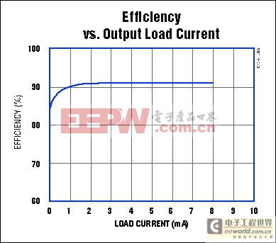
Figure 2. Efficiency in the Figure 1 circuit exceeds 90% for load currents between 1mA and 8mA.
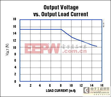
Figure 3. The oscillator frequency in Figure 1, set low to conserve power, also sets a sharp limit on load current.
Figure 1. Consuming only microwatts of power, this 5V-to-15V boost converter provides low load currents with high efficiency.
IC2 compares its own reference voltage against the circuit output, VOUT. The resulting comparator output (pin 8) is high when VOUT is above its threshold and low otherwise. The quad NAND gate is configured as an oscillator, a set/reset latch, and a buffer inverter. The latch blocks oscillator pulses when the comparator output is high. When it goes low, the pulses pass through to Q1's gate and activate the boost regulator.
R4 and R5 help determine the circuit's DC output level: VOUT = VREF(1 + R4/R5). The output voltage ripple for light loads depends on the comparator's hysteresis. With R3 = 2.4MΩ, the hysteresis in millivolts equals the value of R2 in kilohms. Then, the ripple in millivolts equals VREF(1 + R4/R5)(R2), where R2 is in kilohms. For this circuit, ripple = 1.182V(1 + 18/1.5)(1) = 15.4mV.
Figure 2. Efficiency in the Figure 1 circuit exceeds 90% for load currents between 1mA and 8mA.
Figure 3. The oscillator frequency in Figure 1, set low to conserve power, also sets a sharp limit on load current.
模拟电源 电源管理 模拟器件 模拟电子 模拟 模拟电路 模拟芯片 德州仪器 放大器 ADI 相关文章:
- 采用数字电源还是模拟电源?(01-17)
- 模拟电源管理与数字电源管理(02-05)
- 数字电源正在超越模拟电源(03-19)
- 数字电源PK模拟电源(04-03)
- TI工程师现身说法:采用数字电源还是模拟电源?(10-10)
- 开关电源与模拟电源的分别(05-08)