美制造出全石墨烯无缝集成电路架构
据物理学家组织网近日报道,美国科学家研制出了一种新的集成电路架构并做出了模型。在这一架构内,晶体管和互连设备无缝地结合在一块石墨烯薄片上。发表在《应用物理快报》杂志上的这项最新研究将有助于科学家们制造出能效超高的柔性透明电子设备。
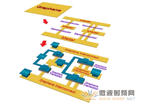
目前,用来制造晶体管和互联设备的都是大块材料,因此很难让集成电路变得更小,而且大块材料也容易导致晶体管和互联设备之间的"接触电阻"变大,而这两方面都会降低晶体管和互联设备的性能并增加能耗。基于石墨烯的晶体管和互连设备极具前景,有望解决这些基本问题。
该研究的领导者、加州大学圣巴巴拉分校(UCSB)电子和计算机工程系教授、纳米电子设备研究实验室主任高斯塔夫·巴纳吉表示:"石墨烯除了是目前最纤薄的材料之外,其还具有一个可调谐的带隙。狭窄的石墨烯带能被用来制造半导体;而宽的石墨烯带是金属。不同的石墨烯带可以制成不同的设备,制成的设备可以无缝地结合在一起,这样也可以降低接触电阻。"
在实验中,巴纳吉研究团队使用非平衡格林函数(NEGF)来对包含有如此多异质结构的复杂电路架构的性能进行评估,并研究出了一种方法,设计出了这种"全石墨烯"的逻辑电路。该研究的合作者康家豪(音译)表示:"对电子通过由不同类型的石墨烯纳米带制造的设备和互连设备的情况以及跨过其接口的情况进行精确的评估是我们的电路设计成功并达到最优化的关键。"
石墨烯研究领域的大咖、哥伦比亚大学的物理学教授菲利普·吉姆表示:"这项研究通过使用一种全石墨烯的设备——互联架构,为传统集成电路会遇到的接触电阻问题提供了一种解决办法,这将显著简化基于石墨烯的纳米电子设备的集成电路构建过程。"
结果表明,与目前的集成电路技术相比,新的全石墨烯电路的噪声容限更高,且耗费的静态功耗低很多。另外,巴纳吉表示,随着石墨烯研究领域不断取得进展,这种全石墨烯电路有望在不久的将来成为现实。
原文参考:
Researchers Advance Scheme to Design Seamless Integrated Circuits Etched on Graphene
UC Santa Barbara researchers demonstrate seamless designing of an atomically-thin circuit with transistors and interconnects etched on a monolayer of graphene
Researchers in electrical and computer engineering at UC Santa Barbara have introduced and modeled an integrated circuit design scheme in which transistors and interconnects are monolithically patterned seamlessly on a sheet of graphene, a 2-dimensional plane of carbon atoms. The demonstration offers possibilities for ultra energy-efficient, flexible, and transparent electronics.
Bulk materials commonly used to make CMOS transitors and interconnects pose fundamental challenges in continuous shrinking of their feature-sizes and suffer from increasing "contact resistance" between them, both of which lead to degrading performance and rising energy consumption. Graphene-based transistors and interconnects are a promising nanoscale technology that could potentially address issues of traditional silicon-based transistors and metal interconnects.
"In addition to its atomically thin and pristine surfaces, graphene has a tunable band gap, which can be adjusted by lithographic sketching of patterns - narrow graphene ribbons can be made semiconducting while wider ribbons are metallic. Hence, contiguous graphene ribbons can be envisioned from the same starting material to design both active and passive devices in a seamless fashion and lower interface/contact resistances," explained Kaustav Banerjee, professor of electrical and computer engineering and director of the Nanoelectronics Research Lab at UCSB. Banerjee's research team also includes UCSB researchers Jiahao Kang, Deblina Sarkar and Yasin Khatami. Their work was recently published in the journal Applied Physics Letters.
"Accurate evaluation of electrical transport through the various graphene nanoribbon based devices and interconnects and acro