Minimal Noise Figure Design
I am currently designing LNA using BFP405 BJT from Infineon at 433.92 MHz. The design goal is to obtain minimal noise figure. During designing I used standard design flow in ADS. Input matching is designed to be optimal GammaS. Everything was fine until I transformed ideal transmission lines into microstrip. The gain lowered and noise figure increased. Now, I can understand losses and thus lower gain, but what happened with noise figure, it shouldn't be affected?
Thanks
Any loss between the signal source and the amplifier input will manifest as both a decrease in gain and an increase in noise figure (typically be the same amount).
If the loss comes before your LNA, this loss is added directly to your overall noise figure.
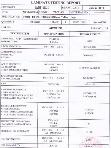
The problem is obviousely loss between input port and transistor. I tried with changing loss tanget parameter, and with lesser losses performances were closer to the performances of network with ideal lumpeds. Tangent loss for specified FR-4 substrate is 0.027 (tested), and <= 0.036 @ 1 Mhz, so I suppose that it is too high, and wonder what would happen at 2.4 GHz, nothing would left of the signal?
Here are specifications of used laminate:
These values are fine for FR4.I guess that you made an error while calculating MS dimensions because @433MHz FR4 can be used without any problem.
FR4 can not have very high loss at that frequency and it may be even used @2.4GHz with a slightly more loss.Check discrapencies between ideal circuit and layout.There should be another missing point.
As was stated FR4 should work fine at 433MHz, with no added major losses to affect NF.
The biggest issue happened when convert ideal TL to practical uStrip. Doing this conversion most of the time appear in the circuit a spread of impedances vs frequency and the circuit needs re-tuning, and sometimes needs to adopt different topology of the matching network to be able to "shrink" the impedances on the Smith Chart.