Simulating thin film resistor in ADS
I have encountered a problem with thin film resistor simulation, and I hope someone could give me a hand on this. Thanks in advance!
It's a simple design with TFR and microstrip, but simulation results from schematic and layout are quite different, I checked several time but I couldn't find any inconsistency in the settings, so I'm wondering if that is "normal"?
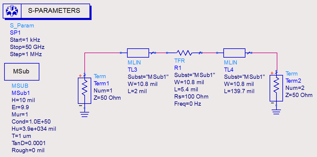
Schematic, layout with substrate settings, and s-parameter results of both simulation are attached. BTW, I checked with someone working on the fabrication, and I was told that the resistance layer has little impact on the simulation (Titanium, 20nm of thickness, and 100-Ohm/sq), thus it can be ignored, is it correct? But no matter how, the "substrate" of TFR in both designs are identical, thus this result was totally unexpected. Any clue?
Thank you,
Mario Young
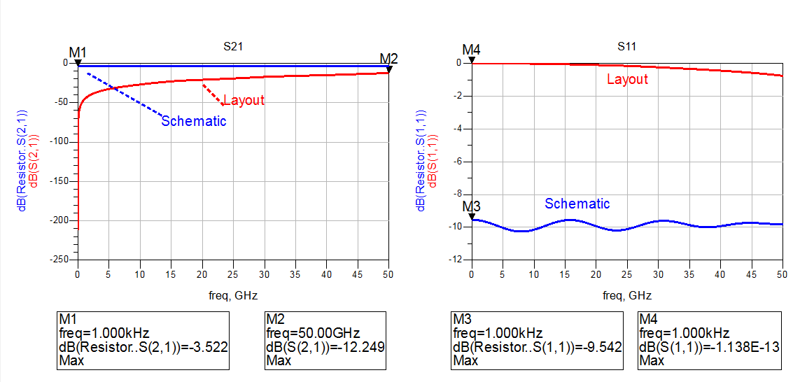
Looking at the open circuit at low frequency, it seems that your resistive sheet is missing in the Momentum model. Have you mapped that layer in the Momentum stackup?
Yes, I didn't add the resistance sheet, I thought it could be ignored. However, I tried with the resistance sheet added, but the results are similar. But I'm wondering if there is anything wrong with the settings, thus I'm also posting it here.
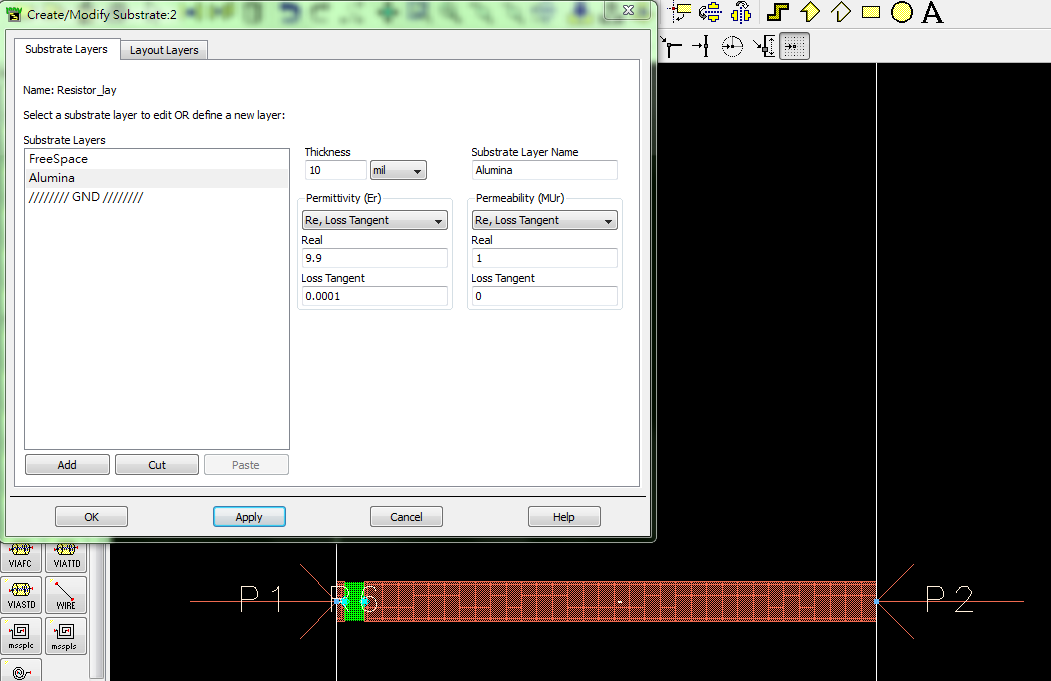
BTW, there is something that I'm confused, in thin film resistor property, the "substrate" refers to the circuit substrate (in my case, the alumina) but not the resistance sheet, right? The schematic and layout that I attached, both of them have TFR substrate assigned to Alumina.
If you leave out the resistor metal, where can the current flow?
You need the resistor metal to represent the resistor -OR- you have to place ports and include it through a schematic element.
Your stackup is wrong. The easiest way to get the correct stackup is this:
Momentum > Substrate > Update from Schematic
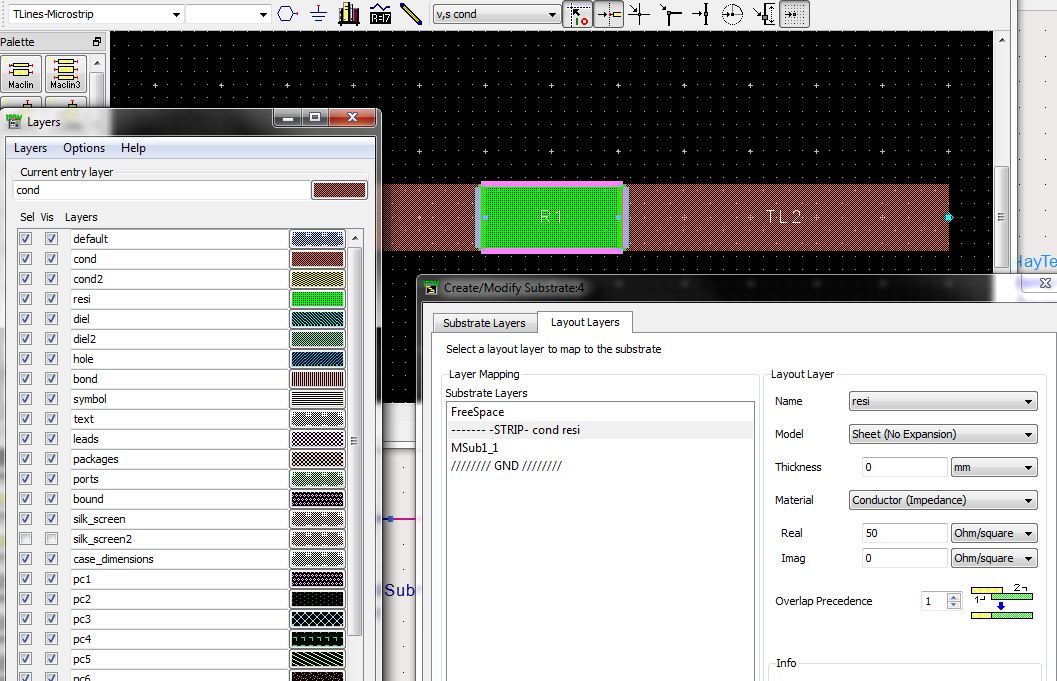
This will create the correct mappings for the line metal (layer cond) and the resistor metal (layer resi)
Both go the same z-position in the stackup. In the Momentum substrate editor, you can check the mapping for both layers:
The cond metal for the line ....

... and the resistor (layer resi) mapped to the same z-position. In my example, the resistor has 50 ohm/square. The value was automatically imported from the TFR element.
I cannot run the Momentum simulation because I have no license, but I am 99% sure that this stackup will work.
Thanks a lot volker! Yeah~ it works :)
Hi volker,
Sorry to bother you again. I have a similar question here, adding ribbon in the layout. I assume the ribbon's layer should be also defined as thin-film resistor did, but apparently the results seems not right, could you give me a hand? I defined "bond" (overlap precedence 0), "cond" (1) and "res" (2) all in the same strip, where "bond" and "cond" are both set to "thick conductor".
Thank you,
Mario Young
Hi Mario, can you show a screenshot of the layer mapping?
Here you have it:
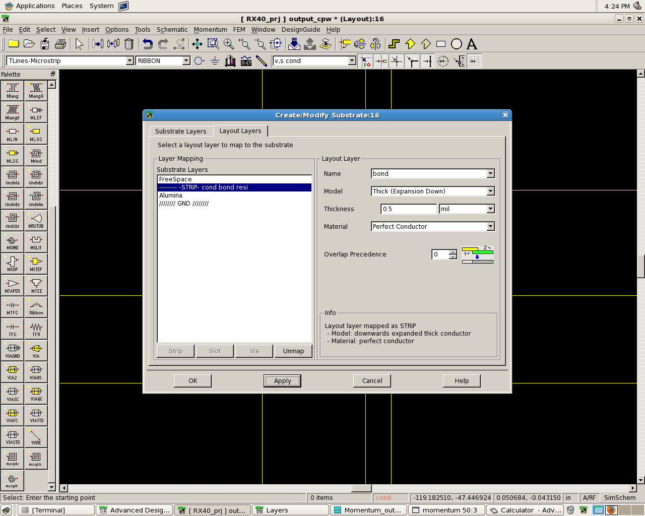
The overlap precedence is: bond (0) -> cond (1) -> res (2)
Ok, so you want all three metals to be at the same z-position? No airbridge/underpass?
Only bonding wires... does it imply that I need to define another substrate, in case air, on top of the alumina, and make another "via" between "bond" and "cond"? I'll try this way. Thanks!
Yes, exactly.
great! thanks a lot!
Thanks Volker... it also helped me!
With Regards,
Vivs
thin Simulating film 相关文章:
- Impedance mathing s2p file in ads
- thin microstrip calculator mismatch
- Thin Film Resistors for Broad band Applications
- Doubt regarding on the Thin Film Resistor(TFR) in ADS
- Any drawbacks of using very thin lambda/4 open microstrip line in harmonic filter?
- Smoothing DC Voltage and inject into RF Cable