Broadband Drain bypass bias for power amplifier
时间:04-06
整理:3721RD
点击:
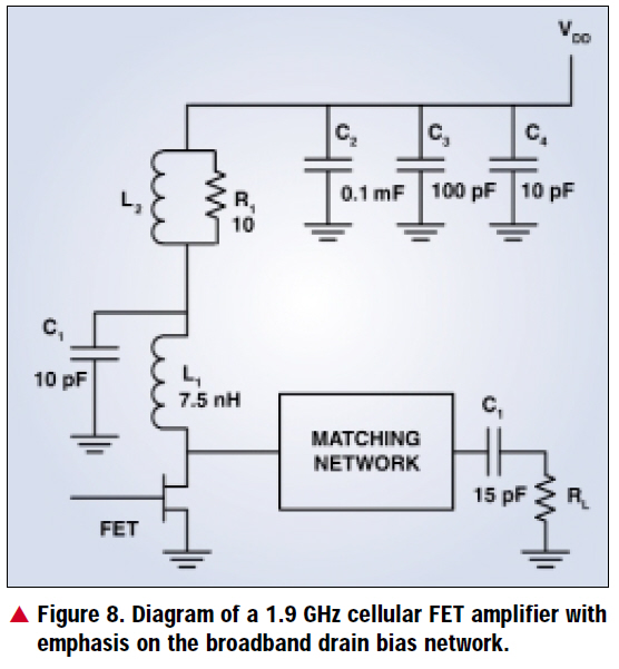
I come across an article on broadband drain bypass bias network. See attached schematic (Bias schem).
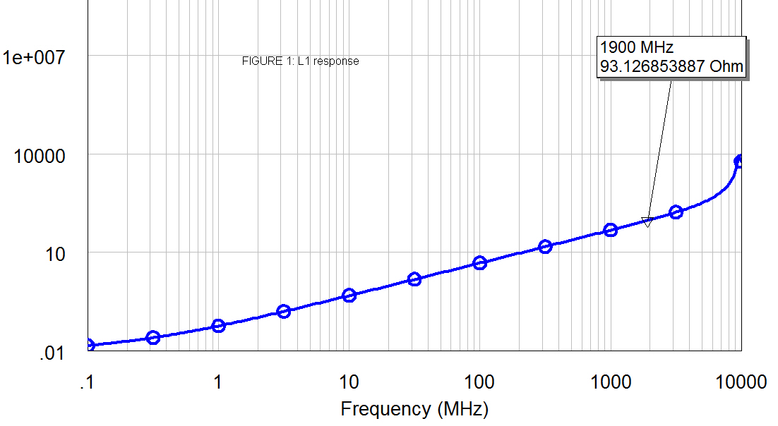
I understand that Z(L1) should be at least 10X the Z(drain) and Z(output matching) to avoid loading the matching. A 7.5nH inductor should be able to satisfy this at RFcarrier of 1.9GHz. See its Z(L1) plot (Figure2) from MWO (the other end of the inductor is grounded in my simulation).
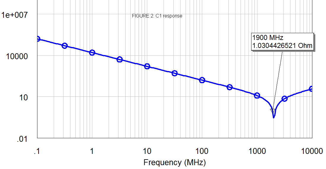
C1 acts as a RF short at 1.9GHz such as to further bypass the carrier frequency. See its Z(C1) plot (Figure3).
Seems to me that everything is fine if we treat L1 and C1 independently.
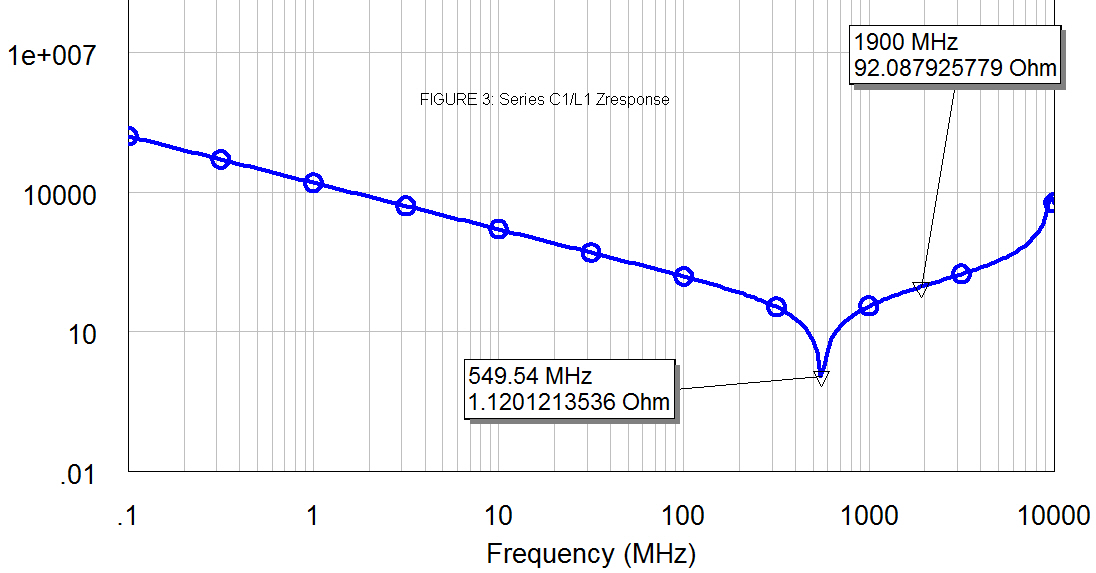
However, if I now simulate the Z looking into L1 in series with C1 (I removed the rest of the circuit), of course the resonance is now shifted at around 1.3GHz, although the impedance at RFcarrier is still high at 1.9GHz.
My question is, should I analyze the Z per component and not the effective Z seen looking into the drain bias circuit?


- Distributed amplifier : What is the purpose extra line at the drain
- GaN amplifier drain to gate voltage
- Drain to bulk breakdown voltage
- Negative voltage for drain in class-E power amplifiers
- Using optimization tools to optimize Drain Efficiency in a Class-E power amplifier
- SKY65116: lower drain when in antenna
