Shifting measurement refernce in s parameter measurement
I want to find the s11 of my on-chip power amplifier output (2.4 GHz) which comes through IC pin. It is followed by off-chip matching network followed by a T line of Zo=50 ohm.
I want to replace matching network with a short and find s11 of the PA. From s11 I want to conjugate match it. How can I move the refrence plane to the IC pin near DUT? I have R&S ZVA
There are basically two options:
- simple port extension. Specify the length of a 50 ohm cable from reference plane to the DUT. Adjust by matching an open or short with the right phase.
- perform an SOL calibration for a reference plane at the DUT, using a 50 ohm chip resistor as load. Usually the more accurate variant, despite of calibration imperfections.
S11 measurement of a power amplifier output is however difficult. It must be performed with the PA in operation, preferably sending a carrier of the intended level.
Load pulling is often a more practical way to determine the output impedance.
Hi FvM,
Thank you for the reply.
1. I want to perform the SOL cal. But in the VNA you should mention the kit name which in my case will be custom since I am using 50 ohm chip res. What kit name shall I choose? Also, I have used 85052D cal kit for VNA. Shall I enter it as 85052D?
2. Is it not sufficient to DC bias the power amplifier and measure S11. Why is it necessary to send carrier? If I send carrier at 2.4 GHz, -10dBm level, should I change channel base power of VNA to -10dBm?
Doing as FvM says is perfectly good, I just want to add that I have a software, AnTune, that is designed to aid with exactly this kind of job.
It is a software that connects with your VNA and live calculates a matching network.
It have smoothing and averaging which can be needed if measuring an active transmitter.
Semiautomatic port extension is also inbuilt, with in many cases improved result comparing to using in VNA existing port delay which in worst case only is doing phase correction.
Supports conjugate matching between two irregular impedance curves.
Automatic calculates best network topology for ideal or lossy components.
Check how I tune a passive 2.4 GHz antenna with aid of this software.
Hope this not was too much of an ad for AnTune, but it really simplifies this kind of job and it is free to try, fully functional.
Leave a 100pF capacitor on IC pin for decoupling of any DC-bias. Some chips also require external DC bias.
Try to measure on a constant carrier. It is complicated to measure impedance if the transmitter is using time-slots with delays in between.
Check that VNA can handle actual TX power level. It is expensive to blow a port of the VNA.
Avoid measuring via long PCB transmission lines as it always adds impedance errors. Forget assumed ideal 50 Ohm traces at 2.4 GHz with PCB in FR4 material. Using in VNA inbuilt port extension is then not enough.
AnTune have functions to correct for lossy transmission lines but in place calibration is always to prefer.
When doing in place calibration, do not use calibration parameters that adds an offset for "Open". Most calibrations standards adds an offset and a assumed fringing capacitance.
I am actually right now doing a matching network and as it maybe clarifies some of your questions is the job documented with some pictures below.

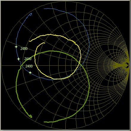
Red is transmitter impedance, powered on but inactive. Green is active TX with carrier at a fixed frequency. Yellow is same curve as green but a bit filtered.

Blue is Antenna impedance. Green is antenna conjugate generated by software. Yellow is TX.
Yes it do probably sucks as antenna, but it is beyond my control.

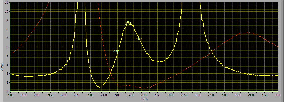
By software calculated VSWR results.
Yellow is TX VSWR relative antenna before matching. Red is after a matching network is inserted.

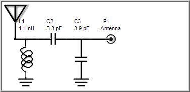
Matching network. Inductors based on Murata LQG15HS.
Verified result with real components was very close to by software predicted curves. Not perfect but as good as it not was any idea to do any fine adjustments. Sometimes must a value be adjusted a step up or down, mostly due to less careful calibration or unexpected losses such as less ideal RF ground.
This kind of matching, from calibration of VNA until finished job, did take me 10 minutes and it is 90% soldering time for measurement cables and verifying result with real components.
Sometimes do these 10 minutes also includes development time of an antenna, as could be seen in the video from my link above.
When I was fresh as antenna guy (many years ago), was a complex conjugate matching at least a full day job, importing curves from VNA to MWO via diskettes and then start a guessing game what the best topology could be and numerous iterations with soldering components and repeated measurements. In best case was final result a minor improvement.
It clearly depends on the amplifier. A linear (class A) amplifier should be O.K. with just the DC bias. This can be expected e.g. for wideband WiFi power amplifiers. The PAs used with FSK small radio devices have often nonlinear and level dependent output characteristics.
Thank you Fvm and E Kafeman for you help.
Hi FvM,
Is it OK to choose any kit name while doing SOL calibration with a custom short, open and 50 ohm chip scheme? I am slightly confused in this regard. There is no option for cutom cal in the vna.
I presume there's an option for an "ideal" calibration reference. If not, you should be able to define it. Practically, the differences between predefined calibration kits should be small related to your measurement problem. You can always check how your calibration is reproduced.
measurement Shifting parameter 相关文章:
