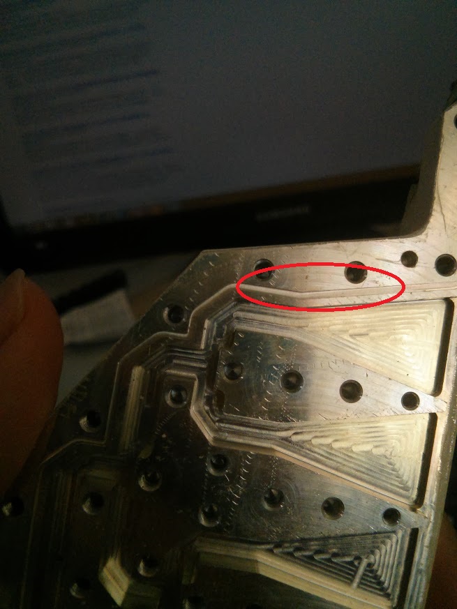
Need help on reducing waveguide leakage
I'm designing a slotted waveguide antenna. For fabrication purposes, the waveguide is split into several parts. However, because of this there is some leakage from the gap between the waveguide parts, resulting in incorrect S11 and radiation pattern. Does anyone here have any suggestions about what I can do to minimize this leakage?
Also, I tried looking into similar commercial waveguide antenna, and it seems that they put some kind of groove on the outermost part of the waveguide. I think that it acts as an RF choke to reduce leakage between the waveguide parts. Can anyone give any reference about this part? I attached the picture of said antenna in this post.
Thanks in advance!

The slot is 1/4 wave length deep. Try wrapping the joints in copper foil. You are using the proper gaskets?
Frank
Hello Frank,
Thank you very much for your reply. Ok, I'll try your suggestion by wrapping the joints using copper foil.
Actualy I'm not really sure about the gasket, since the problem is not about the joint between standard waveguide flanges but the gap resulting from the antenna separated into several parts.
I'll attach the picture of my design here for clarity.
Hard to get the scale but it looks as though the wave guide adapter is only fixed to to the adapter plate via a pair of widely spaced holes. Likewise the radiating plate could do with more fixings down the sides. If the adapter plate (red) is metal perhaps you could drill and tap the narrow "lands"(?) and screw in studs poking out so as to allow the wave guide adapter to be held on with nuts. The ends of the studs in the adapter plate would have to be silver soldered and the slots re-machined. If its not a suitable metal (like Ali), then some form of soft gasket might be needed, but it would require slots machined in the faces at a suitable distance. A bit crude , have you tried to slightly bend the various surfaces, so on bolting down, they are properly tensioned across their mating faces?
Frank
Hi Frank,
Thanks for the suggestions. Sorry for giving proper explanation for the design, but in general the the structure is:
1. Top part (orange) : radiating slots
2. Middle part (red): branch waveguide used to feed the radiating slots
3. Bottom part (yellow): main line waveguide used to distribute power to the branch waveguides
And the antenna is made using aluminum.
I agree that at my first attempt it seems that I didn't put enough fixing bolt so that the structure wasn't properly tensioned. I'll try to fix this problem.
look up the term "split block" waveguide. If you want to make a piece of waveguide in two halves, you split it along the centerline. You do not make most of the waveguide in one piece of metal, and then bolt on a flat cover. That is because RF currents are at a MAXIMUM where that cover would attach, and if there is any surface roughness or warping...you will get high leakage. If instead you split the waveguide half way up the side wall, that is a current MINIMUM, and you can be pretty sloppy about the metal pieces actually mating.
Whoa I just looked it up and yes, it seems that it's not a good idea to make the split there. Since I have structure that's already been made, is there any possible solution to remedy this problem? Or should I just try to rearrange everything?
How about soft-soldering (with suitable solder wire for aluminium) or conductive epoxy?
