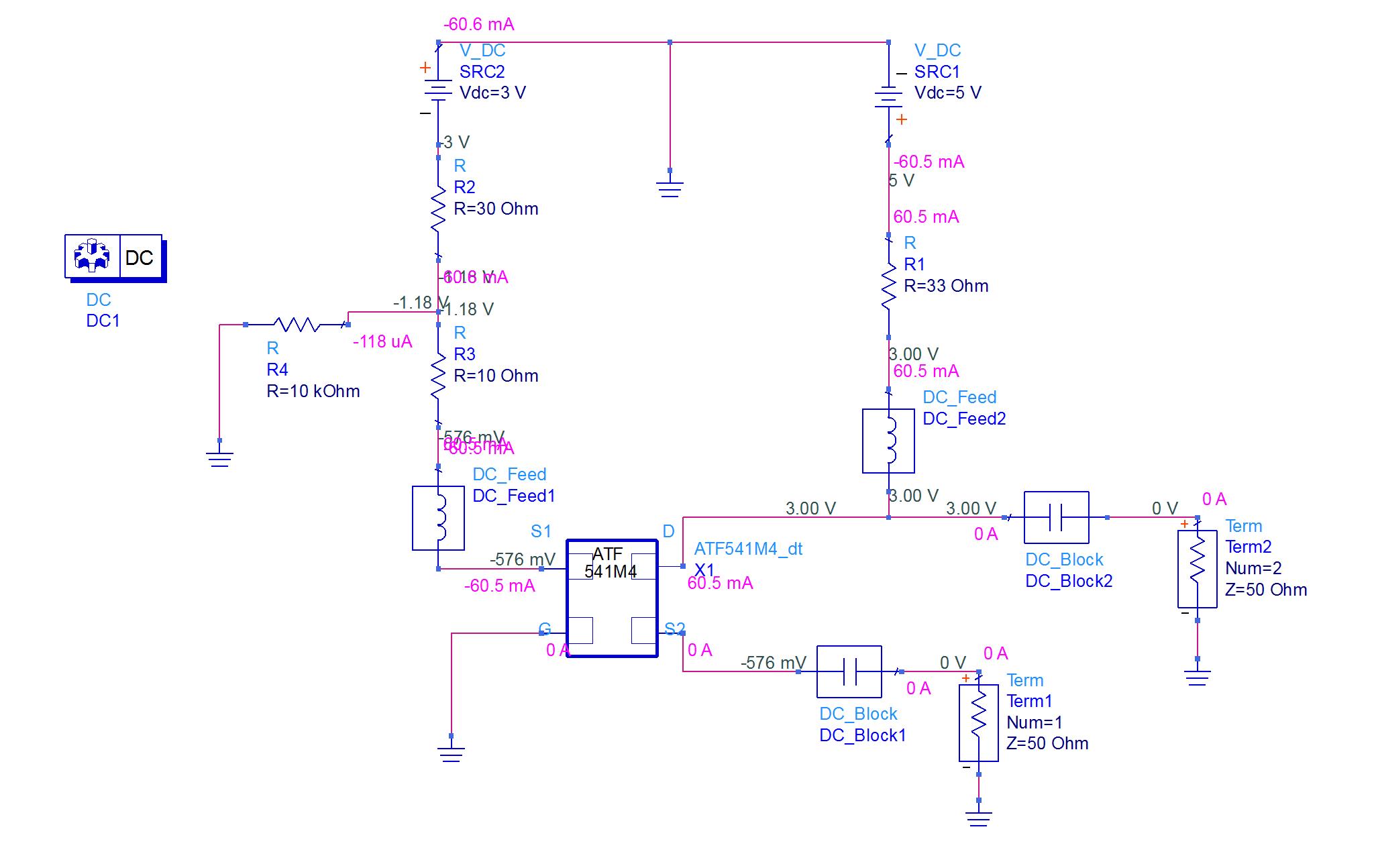
Common gate bias circuit for ATF541M4?
I am supposed to design a bias circuit in common gate configuration.
(using FETcurveTracer template in ADS2011 I found Vgs to be 0.58V in common source config.)
So I designed a bias circuit in common gate as shown in the image.
Is this a correct bias circuit?

The bias should be fine, but in this configuration the gain is about 10dB.
Internally the two source pins are connected together. I have never seen the circuit for a device like this use one of the pins only for dc and the other only for signal. It may work but doesn't look right to me and as I said never seen it done like that before.
Thank you guys for your replies.
@vfone
I am using this transistor bias for designing an oscillator. 10dB gain is good to have right?
@RealAEL
I have used the transistor model package in the simulation. I have to use this transistor which has two source pins after manufacturing the pcb. If we push in to hierarchy(below figure), we can see that these two source pins are parallel. That is why i used one source for dc and other for signal.
Can i use just source S1 for both dc and signal? keeping the other source pin S2 open?
In common source configuration ATF541M4 has about 18dB gain, and most important, has lower noise figure than in common gate configuration.
