Stripline coupler implementation problem
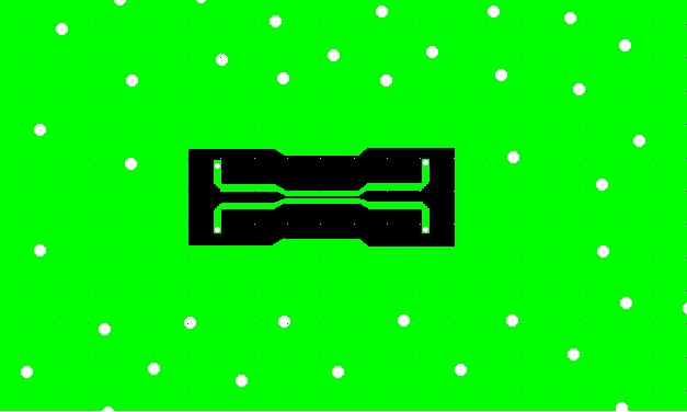
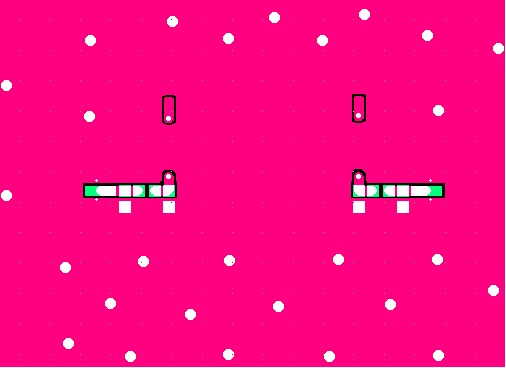
I am new at microwave coupler design. I have designed a stripline directional coupler using Momentum assuming that the upper and lower ground are perfect cover, it worked well on simulation environment. But when I implemented it, I put pads on top ground in order to measure S21, S31, etc.. So I used a transition from stripline to microstrip. But as you guess, it didn't work. The directivity is very bad, the loss is bad. I guess there is a problem with my transition. I put here gerber films and need your valuable comments.
Thank you in advance..
Coupler:

Top ground:

As I observe, you're working at pretty high frequencies( few GHz or more) .If it's true, the distances between input/output pads and Bottom Layer GND are too close.You don't need to lay down GND everywhere on Bottom layer, just underneath of the coupler and around of the input/output lands with a reasonable distance.Vias may be problems,single via might be inductive for high frequencies.
There are somethings to be revised.
Popular errors in EM simulation of couplers: default settings used, without enabling edge mesh, and metal simulated as thin sheet without finite metal thickness. For couplers with narrow gaps, there is also an effect from the solder resist mask on directivity. This can be included in EM simulation if you know the thickness of the solder resist mask.
Popular errors in 2D EM simulation for newbies: consider the ports definition and boundary conditions!
My suggestion is to proceed in two step:
1. consider only the top layer, remove all the ground on top, use ideal bottom ground. Put 4 ports directly on the coupler microstrip. In this way you can verify and optimize the coupler (volker suggestions apply as well).
2. once you get the wanted results in step 1., add ,if necessary, transitions to other layers, modify your stackup and so on.
In this way you are able to understand if the issue comes from some error in the stackup/definition of ports (really a common issue using a 2D simulator with defected ground) or in the coupler geometry itself.
Hope it can help.
Mazz
Thanks for your comments. This is a coupler supposed to work on X band.
Bigboss, about your comments
I couldn't understand what do you mean by saying bottom layer? Bottom layer is not shown here and it is pure ground. Do you say the ground on the coupler layer? I would be thankful if you clarify it.
Do you mean the vias on input/through etc pads? Is it better to put more vias on them?
Mazz, about your comment
You say it is better to design the coupler first as microstrip, see the results, then turn it into stripline coupler topology? And to see all about via effects, ground effects etc, which one is better 2.5D simulation like momentum or 3d simulation like em pro?
Thank you in advance.
Is your coupler really stripline (in the middle between two ground planes) or microstrip?
If it is stripline, you will need many closely spaced vias to connect the top and bottom grounds. In your pictures, there seem to be almost no vias connecting the top and bottom ground. With the vias far away, as you have drawn it, the hardware will fail.
It is stripline.
How far should the vias be from coupler pattern? Can you please show me an example so that I can look at and understand? I need some useful references. I am really new at this concept and need your help.
thank you very much
I hope that others can provide an example for good via placement with stripline. I was never happy with results for my own testcases.
Agree with Volker.
Please add the stackup informations, boards materials. I hope you're working with thin substrates otherwise the vias (signal and gnd) will add lot of parasitics that may destroy the coupler performance.
I didn't mean that you have to modifty the coupler geometry, but you have to be aware about the transition from coupler layer to top layer and, above all, about the difinition of ports in the simulator.
Suppose that you have this stackup (metal layers):
1. Top ground
2. Coupler Layer
3. Bottom Ground
First step make top and bottom ground as ideal planes (boundary), place your ports in the Copler Layer, simulate and optimize the geometry.
Second step, consider real Top and Bottom layers, place vias both in signal path and from TOP to Bottom Ground, modify ports. You now can understand if everything works well.
I hope it can help.
Mazz
Stripline coupler implementation 相关文章:
