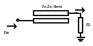
input impedance of coupled line
How can I find input impedance of the following structure where a coupled line is loaded with a load impedance ZL? I have seen this kind of structure are used by people doing filters(as given in pozar). Please tell me how to proceed.
One way I think of may be to write ABCD parameter of coupled-line and that of load then multiply them to get over all ABCD parameter and then evaluate zin from there. But, this sounds a lot cumbersome. A quick way if any to evaluate Zin will be appreciated.
(Note: I don't have idea of image parameter method.) Pardon me for my (as usual) basic questions, again.

Input impedance is function of Odd and Even mode impedances of coupled lines.Therefore you should find these impedances first by calculating or simulating.
You can read something about those in Bahrtia's book.
Couplers are used for frequency filtering (interdigital filters), impedance conversion or directional isolation of signals, or attenuated samples for broadband distribution. e.g. "DC12" gives a 12dB split off an RF trunk. A DC3 could be a combiner or a splitter ( 3.5dB)
Impedance method depends on task. Smith Chart represents changing impedance, Return Loss shows impedance matching and matrix calculations indicate a lump value at one frequency.
For a 3 layer coupler, you might use a method of moment (MoM)-based field solver.
For exploring applications, here are visual images.. https://www.google.ca/search?q=direc...w=1097&bih=543
Thanks Bigboss.
Since I have to find close-form design equations so simulation is not an option for me. In Bahl's book relevant section is here (I will use this structure for impedance matching, too):
What I don't understand here is why have they assumed Zin=Zs, rather than Zin=conj(Zs)?
In my circuit ZL is a complex impedance, will Bahl's method work for me?
the easiest way is using simulation software for you, draw the S11 in smith chart, or check dB(S11)
Simulation not an option for me. I wish to derive mathematical equations by analysis.
they have not made that assumption. use equation 12.13. After that point, they make some simplifying assumptions, that only apply under unique situations.
Also, realize that they are modeling the coupled line for TEM only. Microstrip lines, which are non-TEM, would have a different model. For instance, the electrical length of the line THETA would be different for Even and Odd modes in a non-TEM model.
Thanks a lot everyone especially biff44, for your kind help.
Since I will implement this in microstrip, so this is essentially a non-TEM case. Is there any method to do some kind of compensation to nullify this effect? For instance in one-end joined coupled line, one usually uses stepped coupled line to null the effect of different eve/odd-mode group velocities.
from a practical standpoint, one can load the coupled lines with lumped reactances. If place right, then can work on one mode, but not the other, and tend to compensate. I once saw a paper on trying to equalize even and odd mode electrical lengths by using a sawtooth pattern at the gap between the two lines--in even mode there is not effect, but in odd mode the sawtooth made the lines look a little longer physically.
As I am targeting a dual-band sort of design lumped reactance is perhaps not an option form me, again. Is there link to the paper you are talking about, biff44? How do people working in area of filters do compensation in coupled lines? They too uses these kinds of parallel lines.
- Different Input/Output matching
- How do you choose input power while doing loadpull?
- Why an input inductor required in all GPS LNA?
- Input and output impedance matching in Distributed amplifier
- In distributed amplifiers, is it total input capacitance of the gain stage or Cgs
- curve fitting for input and output matching
