How can I use ATF54143 in ADS2011
I want to simulate circuits in this paper:"http://www.sciencedirect.com/science/article/pii/S1434841112001719".(There is bias circuit in attachment file)
I downloaded ATF54143 from Avago and draw bias circuit in ADS2011,but I get S12 and S21 equal to zero and other parameters aren't like data sheet.I understood The model file which I have downloaded from www.avagotech.com is an old style archived project file and it doesn't work in ADS2011.
I want to get stability factor,noise figure and gain.
can you help me?
Thanks
Zohreh
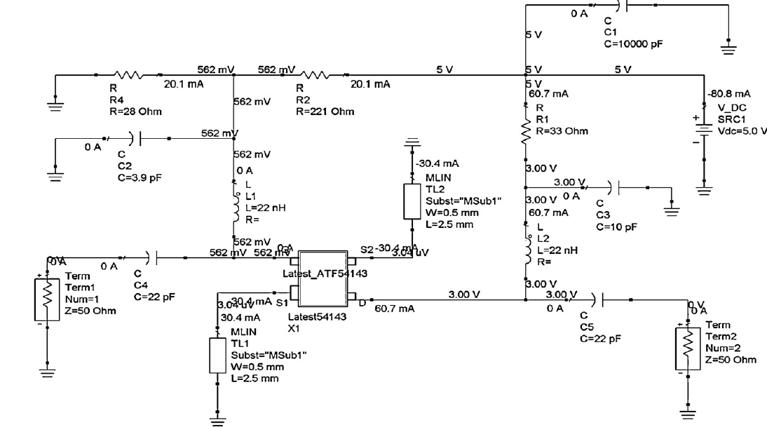
The bias point of the transistor looks fine, why you obtain weird results ?
Model is fine otherwise the bias pioint should not have been right..
Dear BigBoss
Even I changed bias circuit but I got same result(S12 and S21 equal to zero)
I think the ATF54143 block has problem,but I don't know what should I do?
Or is there any thing to replacement of ATF54143?
You have the device connected backwards. The Drain is on the same side as the wide source pin, S1, and the Gate is opposite. You have it wired up with the Gate on the same side and the Drain opposite.
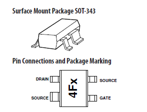
Rotate the symbol by 180 degress and reconnect it.
I don't think so...
I have done the same simulation and the results.can you post your project archive file here ?
I'm using the same symbols as his/her setup but it works.There might be a symbol error but it does not change the pin sequence.
The simulation circuit shows reasonable bias currents and voltages. The transistor can't have gate and drain flipped, it's also effectively impossible that it has S11 identical zero (particularly not with flipped transistor terminals). There must be an elementary fault in simulation setup, not visible in the schematic.
Sir
I sent my archive file.I have used the bias circuit in the paper and it's different with your circuit
thank you
You have attached only the sch.oa file. That is not sufficient to examine the design. You would need to archive all required cels in the workspace or the entire workspace for this purpose.
It wouldn't work.
File-->Archive Project and it will create a *.zap file and post it here..
Hi,
Avagotech website has S-parameter files for noise factor for ATF-54143.
Just download it and RUN in the ADS.
Link is,
http://www.avagotech.com/pages/en/rf...fet/atf-54143/
thanks all
I sent the entire workspace file in the attachment.
You don't have model of the transistor, it's just a symbol...-))So there is no circuit to simulate at all..
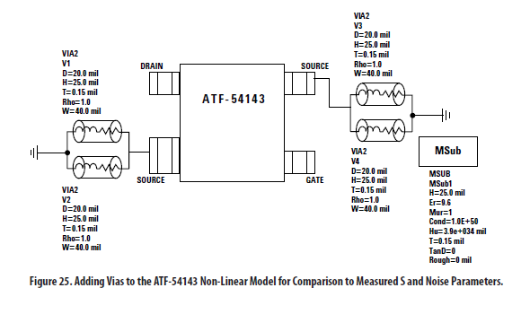
Download Design Kit of ATF54143 from www.avagotech.com and and install this design kit by unarchiving the file which you have downloaded.It's a project file and not a real design kit and it should be opened as project file after unarchiving.It will come as a subcircuit of this project and it's accesible from project library.
then prepare a test schematic and call this sub-circuit onto your new schematic and connect other peripheral componenets them do your simulations.
You have deleted the model schematic for the transistor. The cell named ATF54143_dt should be the equivalent circuit for the transistor that you then place the symbol for in a different schematic to create your design.
Dear BigBoss and Dear RealAEL
I got it.Thank you so much for your help.
Hello
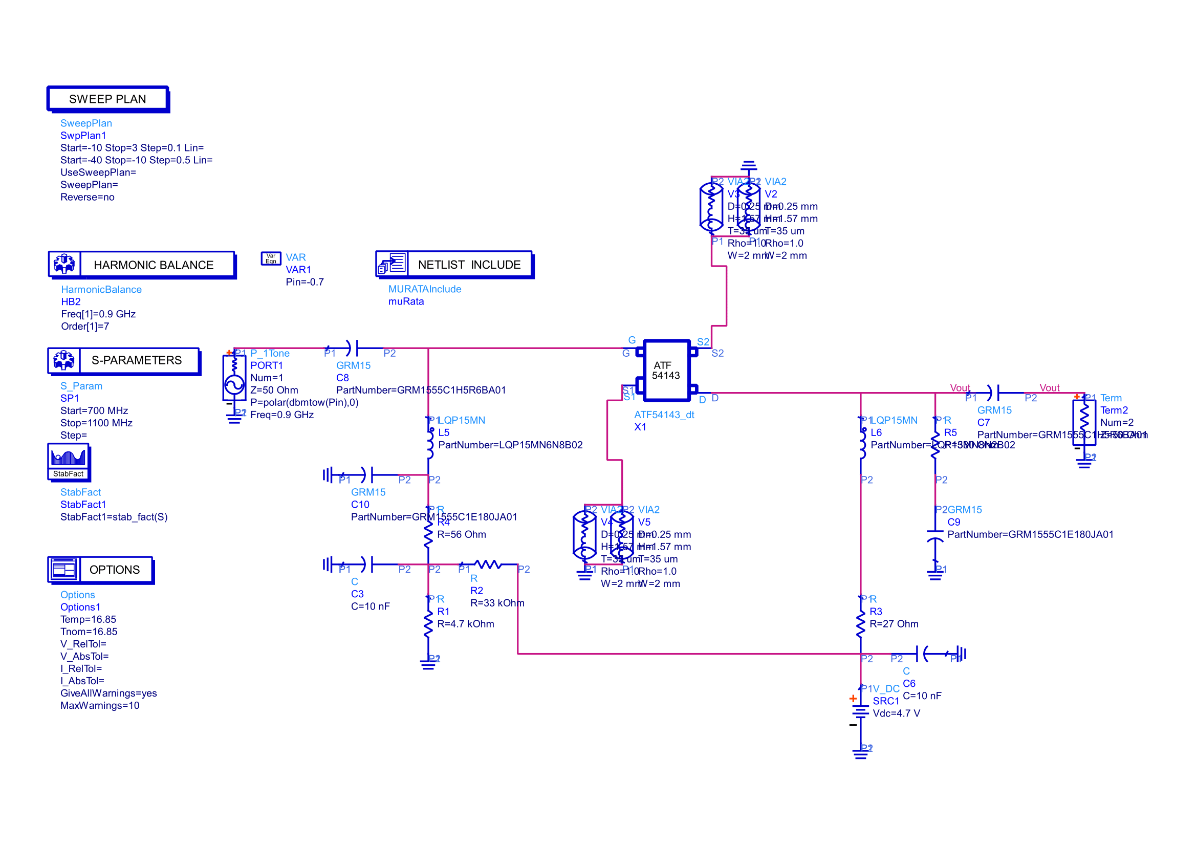
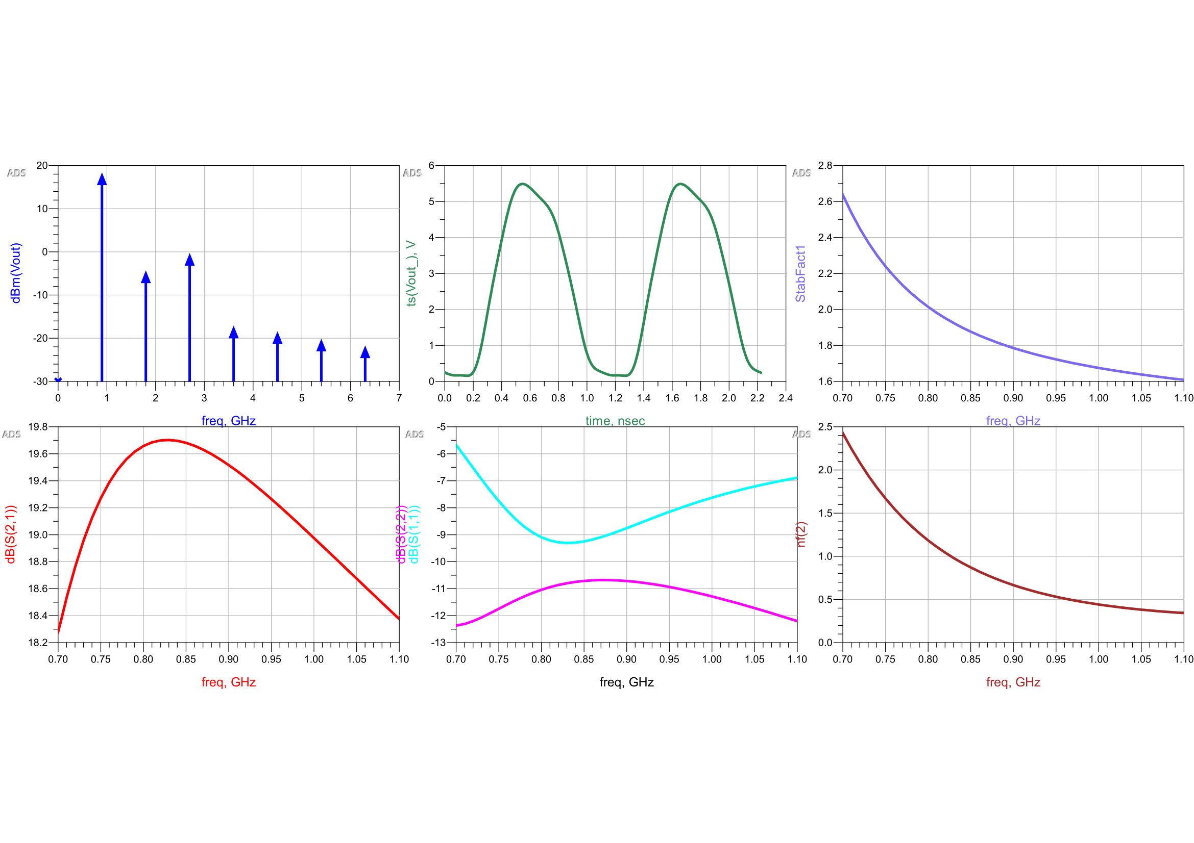
I want to simulate the balanced amplifier in the attachment paper.I simulated the bias circuit of ATF54143 and got good results.when I use it in balanced amplifier,gain and stability factor are good but noise figure and S11 and S22 aren't like the paper results.Even I changed the value and temperature of resistors and matching circuit elements but can't get good results.I don't know what's the problem?.Do I have an elementary fault?
I sent my project archive file in the attachement too.
Thanks in advance.
-Check you schematic because you forgot to connect some matching components to GND..
-Substrate is very important and it has to have at least 0.8mm heigth with Er=4.4-4.6 and TanD=0.05 as FR4 but we don't know exactly which substrate they have being used.
-The final schematic may not be as shown in the paper because I couldn't catch the same simulation results.there might be some tweaks..
I think so....
Thank you sir...your answers were so helpful