Help with the design of BJT feedback oscillator
时间:04-05
整理:3721RD
点击:
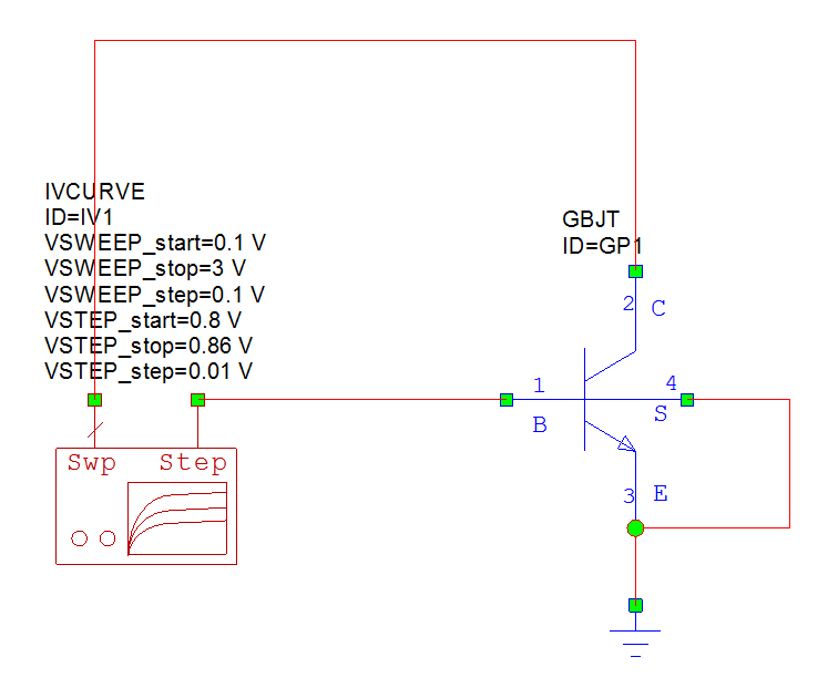
Fig. 1. Setup for IV Curves
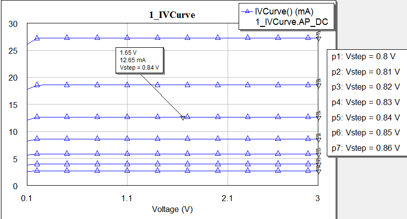
Fig. 2. IV Curves
First, I chose o.p. which is 1.65V Vce and 0.84V Vbe.
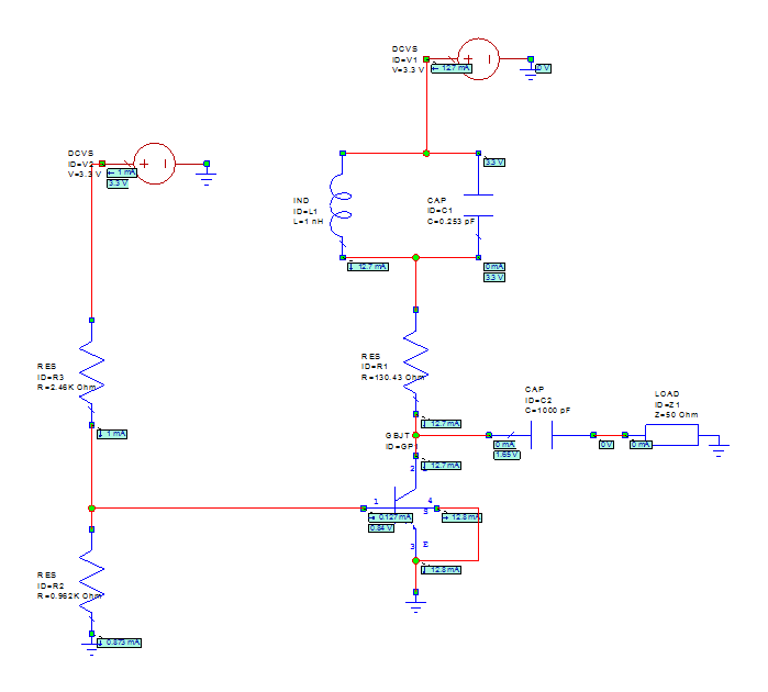
Fig. 3. Biasing Circuit
Then carefully construct necessary biasing circuit for the initial o.p.
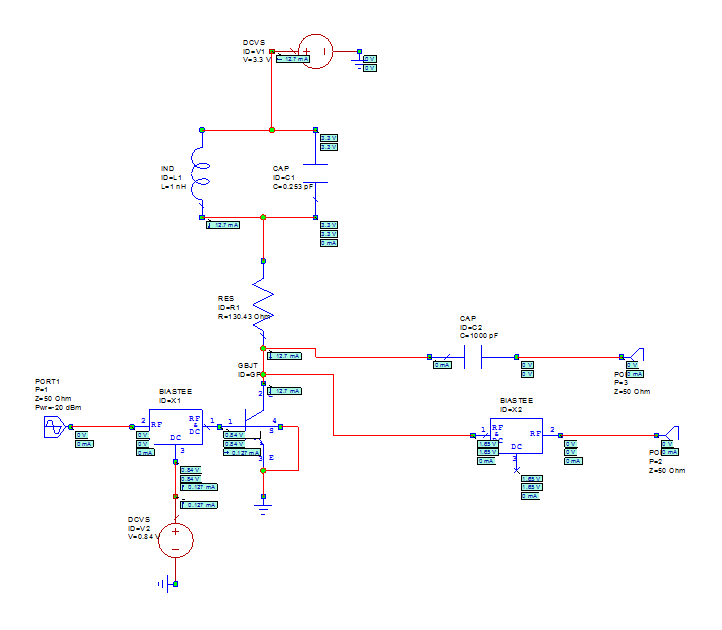
Fig. 4. Setup for VGain, PGain, Phase and output impedance
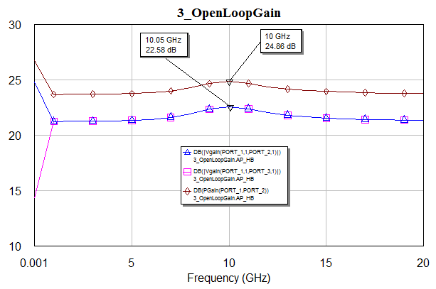
Fig. 5. Voltage and Power gain
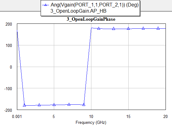
Fig. 6. Gain Phase
I read Voltage gain, power gain and phase change over frequency as seen. As you see, Vgain at 10 GHz is 22.58 dB and RGain is 24.86 db for -20 dBm input. So for -20 dBm input, output will have 4.86 dBm.

Fig. 7. Setup for Feedback circuit analysis
Begin to synthesis feedback circuit. As you see, I have voltage and power gain measurement right from Transistors collector not after decoupling capacitor. Because, input of the feedback circuit will be collector. I cared 2 things through design, 1: very high input impedance, 2: -24.8 gain with 180 degree phase. Of course, I added, the output impedance of the FB circuit which is Transistors input imp in parallel with the biasing circuit. And it came out 186.441 ohm as you can see on Fig. 11.
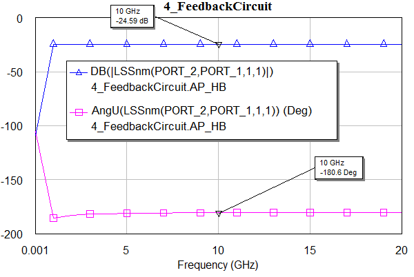
Fig. 8. Feedback circuit gain and phase to the input of Transistor
After a little configuration, I managed to achive desired phase and gain on feedback circuit. Calculation was simple, (Vin + Vout*FB)*(-gm*Rout) = Vout, So Vout(1+gm*FB*Rout) = -Vin*gm*Rout,
Thus, Vout/Vin = (-gm*Rout)/(1 + gm*FB*Rout) therefore, FB should be -1/(gm*Rout), and it means, -24.86 dBm gain with 180 degree phase.
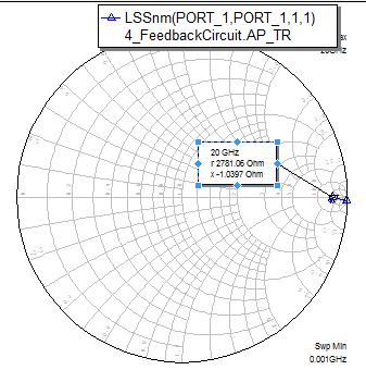
Fig. 9. Input Imp. Of Feedback circuit
Considering FB circuit should not affect Rout, input impedance of the FB circuit should be large so I begin to synthesis circuit with 1K ohm and as you see on Fig. 9, input imp is 2781 ohm so not affecting Rout of the transistor and also gives exact gain and phase I need.
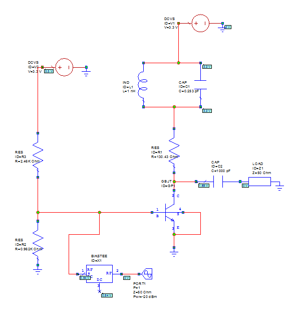
Fig. 10.Setup for Output imp. Of Feedback circuit
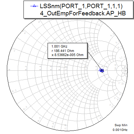
Fig. 11. Output imp of Feedback circuit
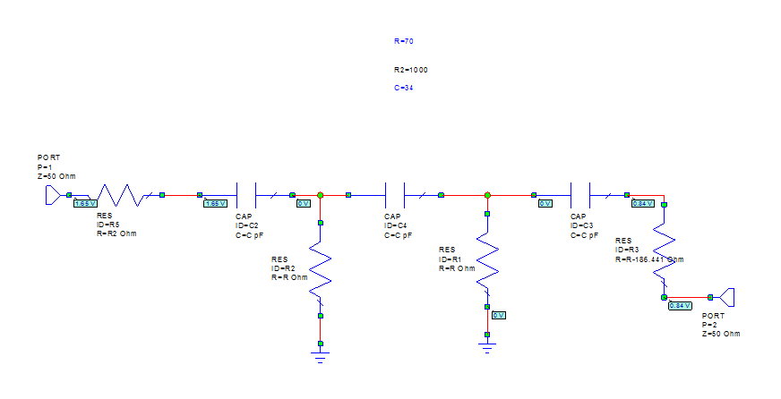
Fig. 12. Prepare the feedback circuit as a block to use in simulations
After I manage to achieve desired gain and phase out of FB circuit, I removed the output impedance and connect the port 2 directly to end of the FB circuit so it will be ready to use as subcircuit. Then I implement the FB circuit for time domain test as you can see on Fig. 13.

Fig. 13. Last simulation setup
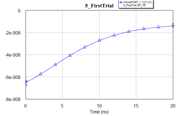
Fig. 14. Time Domain analysis of output
Unfortunately, results were pretty painful. And I am going on a circle for two days have nothing to go on from here. Where did I go wrong? I would appreciate any help. Thanks.
