Component Recognition Request (Amplification at X-Band)
Hi friends!
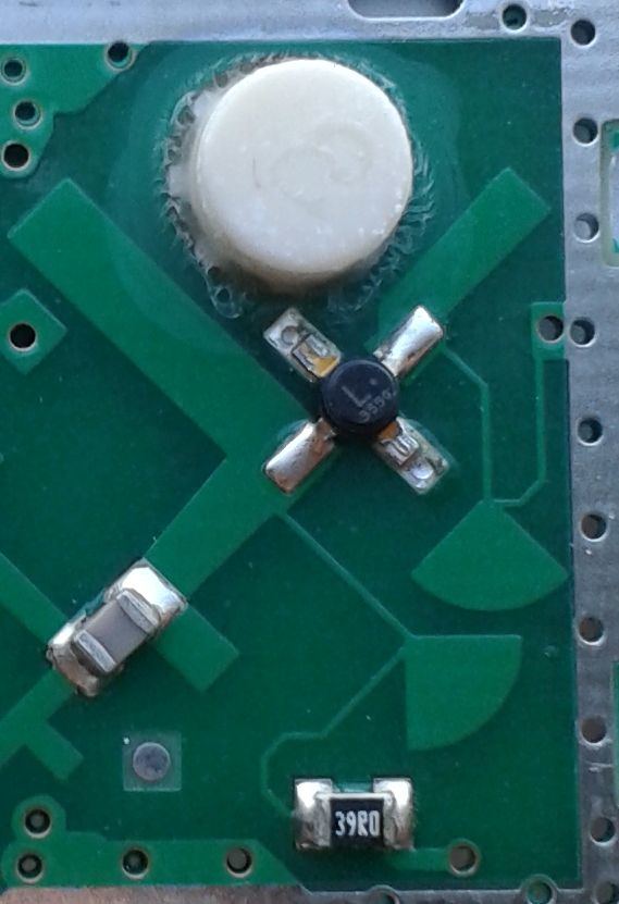
Does anybody recognize the component in the picture? I guess it is a MMIC amplifier but I have no idea about its manufacturer. I could not read its label, it is like L 9550 or L 9S50... search with these words did not make me find something related.
The circuit is part of the low cost microwave motion detector sold around S4. The operating frequency is 10.525 GHz and I guess the amplifier there should provide 10 dB or higher gain. It is active part of the DRO, it compensates resonator loss and sustains oscillation, right? What do you expect its gain? If I want to replace it with a different MMIC, what would be the selection criterion? Gain, phase at op. freq etc.?
It is quite interesting to me to see amplification at X-band in such a low cost module.
Sure looks like a MESFET ( a Metal Oxide Semi FET which uses a Shottky diode instead of PN junction for the Gate, giving microwave bandwidth.)
PLease correct your part number
I see L355C
C or O or 0 or ?
not L9550
Read this for now.
http://www.mwtinc.com/cat/fets/pdf/mwt-1.pdf
I can't trace the exact part but from the layout I would suggest it is either a bipolar transistor or more likely a GaAs FET. I would think it unlikely, although not impossible, it's a MMIC, most DRO oscillators use a single transistor.
A possible candidate is the NE32984D which is an X-band FET with SMD code 'L'.
Brian.
Thank you for the answers.
I can not correct it because I can not read its label at all.
I do not have microscope yet, the most clear vision is in the picture in the first post.
I had supposed that there should be biasing components around its gate/base if it is a transistor. There is only one L(microstrip-conical shaped) to the ground at its gate biasing the gate at 0 V DC. Therefore, I ended up with MMIC guess. I accept that it is a poor reasoning.
Thanks to your posts, I have just realized that some transistors may not require positive biasing to provide gain such as depletion mode transistors(?)
According to biasing shown in the picture can we say that it should be depletion mode transistor? As far as I see, the devices you mentioned look to work with the shown biasing.
They both specify the parameter "pinchoff voltage" as -2V for the GaAsFET and -0.7V for NE32984D.
I have found some GaAs FET devices to be candidate for replacement: ATF 26884, MGF4914D, MGF1801B, MGF1601...
Thank you for your valuable contributions, further elaborations will also be welcome.
It's a D-Type ( probably ) GaAs MESFET DRO Oscillator...
With other active device you probably will need to alter dielectric resonator position. Or add thin copper foil pieces above feedback lines to alter phase.
I replied to you in personal message. Here is some additional information on used FET (NE4210S01 for your photo and ATF-36163 on yellow PCB). I am very interested in DRO's and microstrip resonator oscillators. I have disassembled several X and K-band sensors (10.525, 24.125 and 24.150GHz). Actually i was trying to learn using this approach: First, i can calculate biasing of real design, see what resistors are used. Then i can see what Q-point and load line is, and what S-parameters are for this biasing. Second, i can see what matching was performed, length of phasing lines, stubs, etc.. Mainly i use QUCS, SPEQMATH and SONNET LITE for learning. I simulated S53MV's narrowband oscillator in Sonnet Lite and QUCS, got zero phase and amplitude maximum for 2.256GHz for quarterwave short stub resonator with phasing lines and BFP420. I think this learning approach is very nice, when you step by step learn how real device works. Not some abstract numbers. Here some sensors i learned:
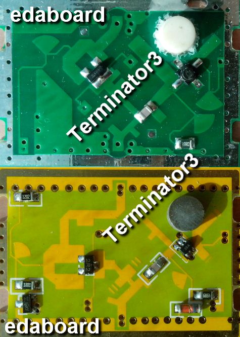
Transistor you searched for is surely NE4210S01. You can find datasheet and S-parameters here: http://www.cel.com/parts.do?command=load&idRootPart=457. But on photo above you can see the same PCB(green one) with other FET NE3512S02. There are many similar transistors, and their S21angle phase is differs not very much at 10GHz.
Vd=2v, Id=5ma
NE4210S01 10.5GHz S21angle=42
NE3512S02 10.5GHz S21angle=41
But green PCB have only 39 Ohm biasing resistor, and VCC on the board written is +5V ! DC load line is very steep 5v / 128ma = 39 Ohm, and gate biasing is 0v. I think this oscillator have harmonics at 21GHz. Here is DC load line calculation tutorial i like: http://bear.cwru.edu/eecs_cad/tut_spice3_jfet_bias.html
So what i can"t understand is biasing resistor of 39 Ohm and Id have some crazy value of 128ma, as i understand it is clipped by FET's i-v curves, but DC line is still very steep.
For (Vd=5v, Id=128ma) S-parameters may be very different from Id=5ma biasing.
I tried to calculate parallel feedback angle based on S21angle, but it seems wrong. In theory it must be two microstrip lines. Both lines must have length around (42/2 deg from transistor to coupling point with DR+ 90 deg open stub). As transistor's phase shift is +42deg, lines will give -42deg, so total phase is 0deg. I tried added 360deg, but it becomed obvious that lines are not so long here (green PCB). Maybe phase is changed because of other stub at drain, where 0805 capacitor is placed. Also i found paper, where stated that similar NE32****/NE35 FETs S-parameters are given from the point where pin touches pad. For example, NE4210S01 S-parameters reference plane at 2.4mm diameter (1.2mm radius) from transistor center. Exactly where pad begins.
I did some S-parameter based phase-amplitude simulation for microstrip parallel feedback simulator in QUCS. It all seems well. I used NE3210S01 transistor s-parameters, this transistor can replace NE4210S01 and NE3512S02 and seems easier to find. Here is full list of NEC FETs: http://www.cel.com/product.do?comman...=4&level2=2407
On the yellow PCB is a better design (photo above): first of all, there is diode in glass case. It provides voltage drop from 5v to around 4v, so DC load line voltage is always below FET's maximum recommended raiting. Secondly, here is some biasing resistor for mixing diode. Diodes in all this desings seems to be HSMS-8202. Third, there is additional diode at IF-output of mixer. I guess it protects weak HSMS mixing diode from static electricity. But adding capacitor after that would be even greater. FET used is ATF-36163 (http://www.hp.woodshot.com/hprfhelp/...s/atf36163.pdf)
Here is another one, i found this picture in internet:
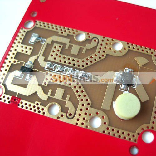
a little strange design where few resistors are connected in series
I think that it is better to use negative biasing IC, because then there is more freedom to biasing, and it is possible to increase/decrease harmonics and shut off unwanted oscillations with more negative biasing. Now such IC is very cheap.
About perpendicular branches, I am almost sure now it is the same as parallel branches. Because magnetic field lines from DR would have the same configuration.
Although i have read some paper, where parallel feedback lines was called as "inverting phase case". Very strange, because phase shift of DR coupled with quarterwave stubs gives zero phase shift, for example in RLC model simulation. But if we put DR as microstrip in band-pass filters (replace half-wave microstrip resonator with DR), there would be a different case that called "non-inverting". I can't understand why is that. Actually i think that parallel feedback is non-inverting, because we get zero phase shift at coupling (current direction is correct), and 180 phase shift for other case.
Hi Terminator3, I thank you very much for your valuable contributions. Actually, I had seen your private message but did not answer immediately. I had planned to study on the topic to make better contribution.
It is nice to see alternative FETs for the DRO.
I think the bias current is not 128mA at all. As you can see in the product(microwave motion detector) description page, the supply current is specified as 37mA typ. 60mA max. I see the current around 40mA in my works. The bias current cannot be calculated by simply dividing the supply voltage by Rbias. Did you overlook the drain voltage? For example if the drain voltage is biased at 2V then the current through the drain(which is bias current also) will be (Vsupply-2)/Rb. Say Vsupply=5V and Vd biased at 2V then I=(5-2)/39=~76mA
I think that simulating the resonator part in an EM simulator is great step in DRO design. If I succeed to get reasonable results in CST, I will share with you to comment on.
Sincerely.
I understand your doubts about 128mA. Here is my explanation to this:
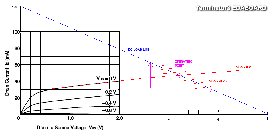
This is I-V curve from datasheet of transistor you searched for. Here you can see that Id becomes almost 130mA if FET have a breakdown or VGs becomes too positive. This current is 130mA because it is limited by Rdrain=39 Ohm. So maximum current through drain-source and resistor is I=U/R=5v/39Ohm=0.128A=128mA.
Also we can see, that Rdrain=39 Ohm is the only biasing used on this PCB, and conclude that Vgs=0v. Now we can find operating point ("Q point"). Vg = 0v, Vd=3.2v. Feedback 10.525GHz signal comes to it with some amplitude something like (-0.2...+0.2v) around 0v. That wil give drain voltage amplitude about (-0.6...+0.6v) around 3.2v, then it goes through feedback line, to output, and after attenuation may be around (-0.2v...+0.2v) again when reaches gate.
Here is picture from tutorial at http://www.electronics-tutorials.ws/ that explains what i mean:
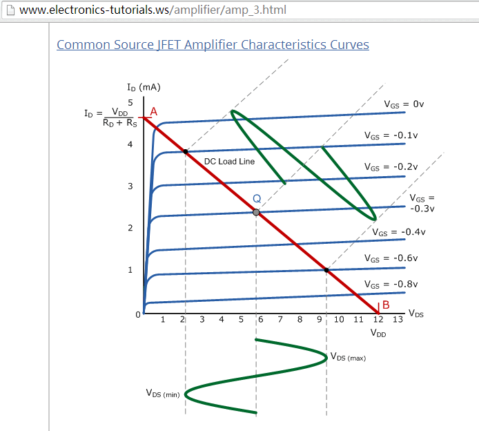
Here you can see, thad Id on load line is calculated as Id=Vdd/(Rd+Rs). In our case we have Rs=0 (no additional biasing to make negative Vgs). And if i understand it all right, then according to this tutorial http://bear.cwru.edu/eecs_cad/tut_spice3_jfet_bias.html calculations are correct.
I want to see how Id vs Vds will be for Vgs greater than 0V. In all datashits and tutorials I-V curve of N-channel FETs is given only for region about 0V to -4V. How it will look like for positive Vgs?
p.s.
it is interesting to see that result of operating point on my image not so far from Id=40mA.
But still, dc load line is steep and can reach 130mA. I think in some cases this oscillator can have some failure, for example if gate have some interference signal amplified, so current will become too high, and it will burn out.
p.p.s.
btw, betwixt suggested that FET is NE32984D. I was curious why it is also marked "L" as NE3512S02. I searched for datasheet. I was confused until found this text "LOW COST METAL CERAMIC PACKAGE". It seems that NE32984D have white ceramic "cap" (white-colored transistor). NE3512S02 is "Micro-X plastic (S02) package", which is black. I think this explains why one manufacturer have same marking for different transistors.
I found interesting 1979's year patent at freepatentsonline.com: http://www.freepatentsonline.com/4357582.html
by Mitsubishi:
Also it is compared to other microstrip arrangements. Here is something about design itself:
Difference with green-pcb is that:
1) output taken from source line.
2) there is termination resistor on gate that works at microwave
3) drain stub is made half-wavelength
Strangely patent states that drain stub is half-wavelength regardless of FET's S21 phase. Maybe i am miss something.
Yellow pcb looks more than series feedback. Although at this frequencies many FETs have very good gain, so even with wrong design it is possible to find DR position to make good feedback.
Red pcb looks more like classical parallel feedback, but DR positioned a little different (no quarterwave-open after coupling point)
It all gives a feeling that this designs are made using prototyping with some hand-tuning, rather than calculations of feedback lines.
I tested green PCB. It seems that sensitivity is a little low. Maybe power output is too low? I use simple inverting OpAmp schematic with gain of 300. But it is less sensitive than my previous test oscillator with monopole antenna and single diode mixer (with same opamp setup).
I made two oscillators on a FR4 1.6mm board. One with classical parallel lines arrangement and other with right angle feedback lines (as on green pcb photo in first image in this topic). I extracted white puck dielectric resonator from the green board to use in my design.
Although i calculated feedback lines length very carefully with use of S-parameters, in reality they must be cut much shorter. The problem with parallel lines arrangement is that it had unwanted oscillations from the beginning. As i made lines parallel, it is impossible to cut it too short, so instead it was made longer. Still very unsatisfactory results, even with wide 50 ohm lines (from what i learned it must give less coupling between lines, as in microstrip filters with wider lines). It may give an idea why on red PCB we can see lines are not parallel. This arrangement can make line shorter and also reduce coupling between lines.
Surprisingly right angle lines arrangement was stable from the start (same biasing, same gate and drain stubs), and with different cutting and adding copper foil. Also adding resonator was much easier, less sensitive to alignment between lines. And oscillations was observed even when resonator was very far from both right angle feedback lines. It seems that on 1.6mm thick substrate magnetic field goes much farther than i thought, and it explains unstable behavior of parallel microstrip lines, where feedback achieved without resonator.
It's my experience young RF engineers over-estimate the dielectric constant of FR4 and thus transmission lines have higher L/C ratio.
This not only raises impedance and lower return loss. It increases leakage and coupling so orientation is more sensitive and Smith Chart stability circles degrade.
Also ground path between conductors can reduce coupling effects of parallel tracks when included in impedance calculations and right angle stubby tracks are most stable.
But I have no experience with this part.
I read California Eastern Labs is now owned Renesas Electronics Corporation which merged and took over NEC division of similar parts in 2010, so you can expect the best new parts will be available in Japan only for a while.
Can we replace dielectric resonator with microstrip ring resonator? Of course Q would be lower, but phase seems to be right only with parallel lines.
Magnetic coupling to parallel lines, phase shift through ring 180deg.
Magnetic coupling to 90deg lines, phase shift through ring 90deg and 90+180deg. So actually it will supress operation frequency. But when we use bigger ring for half of operation frequency phase shift would be 180 deg and 180+360deg (through two "arms" of ring), so it looks like pretty real.
