Any obvious issue with this layout?
I'd like you to have a quick look at the pics and leave a comment...
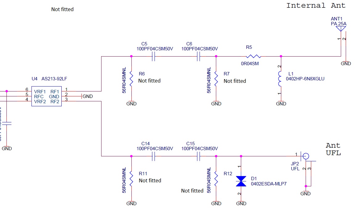

It is part of the RF section of a system with GPRS/3G communication capabilities.
The pcb layout shows a transmission line with a track width that is a bit narrower that component pads connected to it...
is this a good practice?
no significative impedance discontinuities?
U4 pins 1 and 3 connect to transmission lines with a 90 degrees angle...
is that ok?
Regards
well, yeah. the inductor is not returned to a ground plane, but to some length of transmission line.
What are all those resistors for?
To be honest I don't know
Considering that the one in series has value 0R0 and the others in parallel to reference are unmounted, I guess they are there only due to a potential need of impedance matching with antenna by reducing reflection coeficient.
I recommend you to put some distances between the TLs and GND and reinforce the TLs with shielding vias around the track.
The best is to calculate and simulate the layout with EM simulator because layout may change everything regarding to presumed performance.
As was stated you need bigger clearance between the 50 ohms microstrip lines and ground plane.
To be outside of the CPW mode, the distance should be at least 1.5 times greater than the microstrip line width.
Thanks for your responses guys.
What do you think about track width-component pads difference?
Regards