RF/voltage clamp/limiter
I'm looking for a circuit that is called "RF clamp", "RF limiter", "voltage clamp" or "voltage limiter".
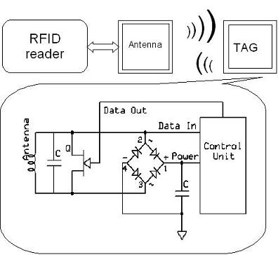
The example of such circuit is a transistor Q on this picture:

However, what I need is a full RF clamp circuit. Not only the transistor shown in the example above. The gate bias of this transistor would be very useful.
I cannot find many of such circuits. Often, they are stacked diodes on antenna lines or diodes + resistor to bias transistor clamp.
Do you know where I could find good examples? Any books, websites?
The circuit has nothing to do with "RF clamp", "RF limiter", "voltage clamp" or "voltage limiter". It's a typical RFID load modulation circuit.
A series of shottky diodes in two back to back strings should do it. We used 7+7 (from memory) to protect from 1W, good to 30 MHZ. The secret is to use a ferrite input and output transformer. The DC current saturates the cores giving lower coupling.
Frank
@FvM
Right. On this picture the gate of the transistor Q is labeled as "DATA OUT".
However, the same transistor, but with different pin connected to the gate may be used as RF clamp.
I chose this picture as it was the simplest, but I didn't notice "DATA OUT" label.
Here may be a more proper example just to show where RF clamp is located :
https://www.google.pl/imgres?imgurl=...act=mrc&uact=8
@chuckey
The problem is I cannot use Schottky diodes. They are no available in CMOS process we use.
To get the best circuit efficiency the clamping diodes should be placed outside of the chip. I remember while ago, we were in a situation when the internal CMOS clamping circuit fails very often, due to a poor chip layout design.
You mean back-to-back diodes? You used internally PMOS diode-connected transistors or p-n diodes?
Finally, you took discrete diodes?
- Induced voltages on transmission line by plane wave in HFSS
- Klystron output voltage, cavity field strength
- Negative voltage needed in K-band
- How to set the bias voltage of the BJT in Gilbert mixer
- is DC voltage gain not an important issue to consider in LNA designing?
- Power (Voltage / Current) inducted in rectangle antenna.
