Voltage multiplier for RF energy harvesting
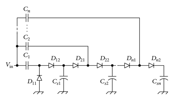
I'm doing an RF energy harvesting circuit in UHF band. My question is about the voltage multiplier. My 2-stage multiplier (using 2 HSMS-285C diodes) follows Karthaus-Fischer's voltage-doubler.
A 0.1F supercapacitor is put right at the output of the multiplier. This DC voltage will be provided to run an MCU and a sensor. The minimal voltage for operation of MCU and the sensor are 1.9V and 2.56V, respectively.
As in theory, the DC output voltage of the multiplier will be:
Vout = 4 * VRFpeak - 4 * Vfwd (forward voltage of the diodes) - Vload . So say, if Vpeak is 300mV, the maximum voltage I will get is 1.2V, ignoring Vfwd and Vload.
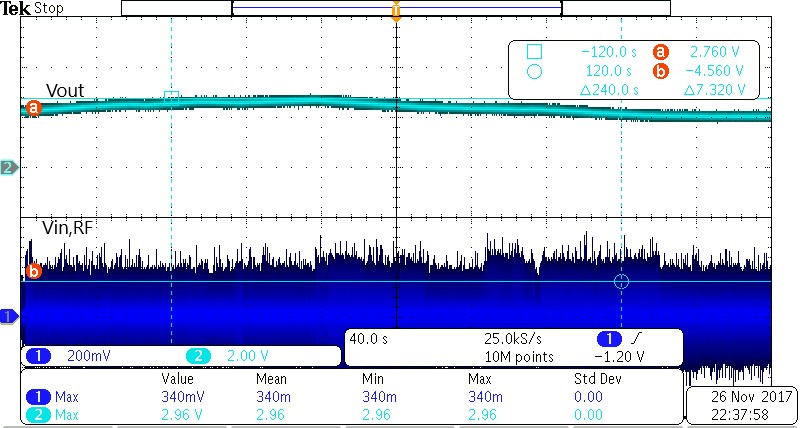
Here is the problem. When I measured the input AC voltage at the receiver antenna (Powercast) terminal, I got a very small signal with the maximum amplitude of 200 - 350mV. BUT I could get 2.6 VDC with full load as told above (MCU & sensor on full operation). Not all the times I could get this result, but sometimes I could. Please refer my picture below.
Probe1: Vin, RF
Probe 2: Vout
Please help me explain this phenomena. It seems my measurements went wrong, or my theory got sth wrong. Thank you very much.
What probe do you use for Vin,RF ?
Dear pancho_hideboo, I was using Tektronix TPP1000 1GHz (Probe 1) and Agilent 10:1 probe (Probe 2; input impedance was set to 1Mohm).
Unbeliebable measurement set up.
Long lead, Cheap probe with more than 10pF.
Do you have sure experience of measuring 1GHz ?
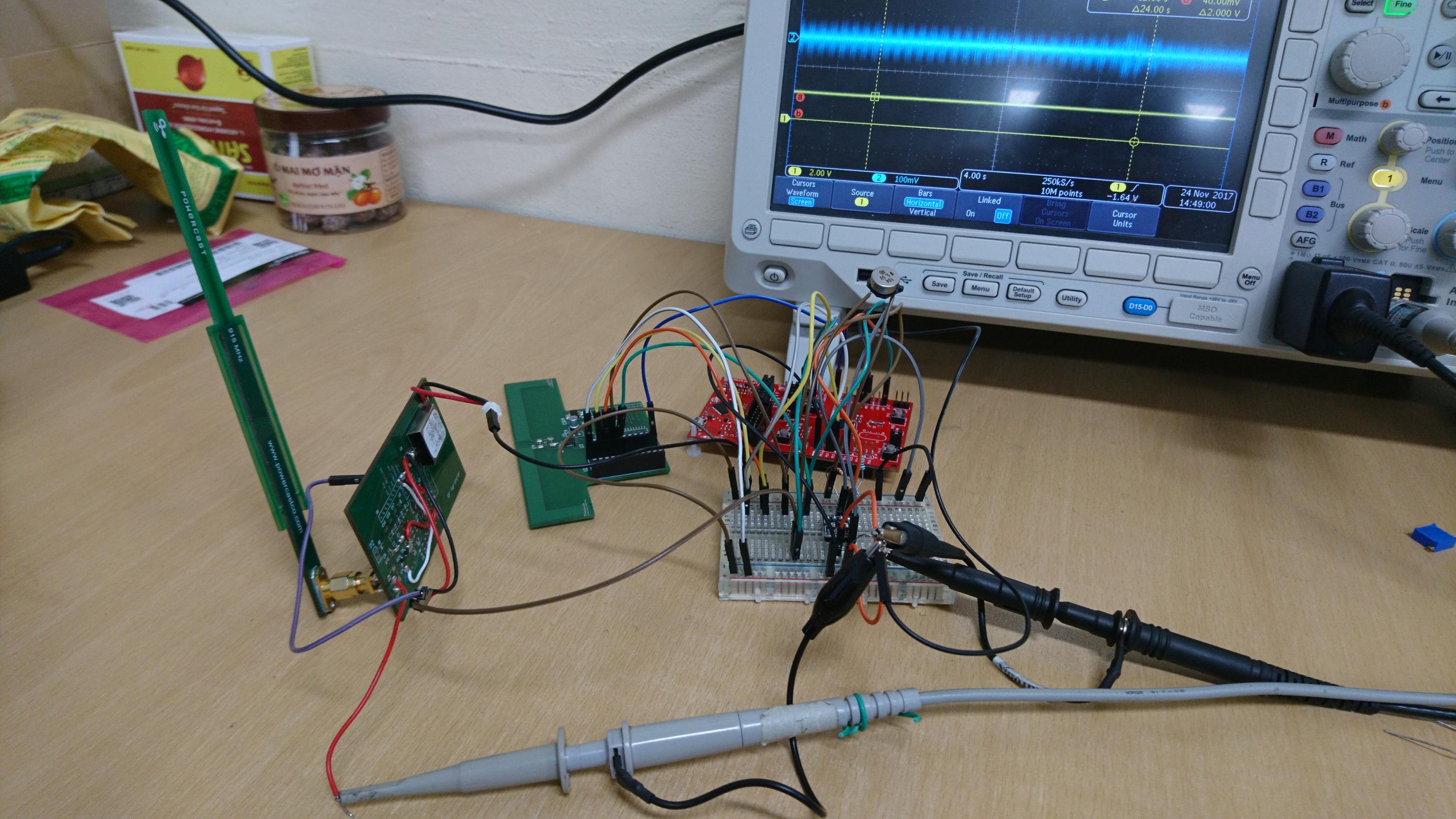
I would estimate the red wire from the RF board to the tip of the scope probe to be about 10cm long. At 0.5mm wire thickness this will give an inductance of the red wire of at least 100nH.
You connected the ground of the scope probe to the breadboard, which is placed at another 10cm distance from the RF board (brown wire). So, another 100nH in series to your UHF signal, practically eliminating any RF ground for your probe.
The strangest of this test setup is the aluminum capacitor suspended at 10cm in the air over the breadboard.
You need to do a lot of readings to understand what means RF measurements.
@pancho_hideboo: Thank you for your comment. I'm new in RF, and I do not have any experience in RF measurement. My analog knowledge is not good either. Yes my experiment set up was so funny, but I did not know how to test my circuit board in modules (harvester module, impedance matching module, load module etc. ). So I designed it into different modules with many jumpers and long wire to test and fix one by one. Could you please tell me where I can get the tutorials for RF measurements or how I can test the RF analog modules as good as possible?
@vfone: Thank you for your comment. Yes I need a lot of readings to understand RF measurements. Regarding the capacitor, it is exactly the supercapacitor I put right behind the multiplier circuit. Because there was no space for me to put it on board, so I had to plug it into the breadboard.
Were you saying that the RF ground practically was not connected to the probe's ground with that set up? Should I connect the probe's ground directly to the antenna ground (although I do not imagine how I can do this without any wire)?
I'm sorry I should add more details in what I'm doing. I'm doing exactly an RFID transponder at 915 MHz. The reader I'm using has the output power of 650mW. At the distance of 15-20cm where I got the result as mentioned above, the received power, measured by a spectrum analyzer, is 3 dBm. The antenna I'm using is a microstrip one with S11 = -(15-20) dBm from Powercast. It's input impedance is around 50 Ohm (measured by VNA).
Please refer to my RF harvester schematic.
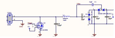
Right now I cannot make the impedance matching circuit (L-type) work. So I currently short the L by a small wire and leave the C open.
What do you mean by "S11=+5dBm" ?
S11 is less than -10dB.
This is contradictory with "S11=+5dBm".
Why can not you achieve impedance matching ?
Here large signal RF matching is required.
Oops I'm sorry for making this confusing. I mean it's around -15 to -20dBm when measured by the VNA.
I cannot implement the impedance matching because the load impedance cannot be predicted. I do not know how to predict the load impedance (including voltage multiplier, charge bump IC, RFID tag chip, MCU, sensors) with different operational states (harvesting, backscatting, sleep, active, low-power states). The L,C values of my current matching circuit are from an existing schematic; they practically, however, do not match my application. Any time I put them there the power received is reduced so much that I could not get the desired voltage.
Keysight Web Sight.
Still you are wrong.
@pancho_hideboo: Thank you for telling me the tutorials. I'll be reading them. And I'm sorry again for my carelessness. The S11 must be in dB.
multiplier Voltage RF 相关文章: