PAE Class-E Power Amplifier Problem
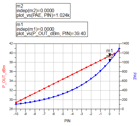
I Already design Class-E Power Amplifier using MMG15241H (freescale : https://www.nxp.com/products/rf/rf-a...sign_Tools_Tab) with the linear model transistor (S2P File) for my final project, the bias voltage is known to be Vdd = 5 Volt and Idd = 85 mA but when I tried to calculate the PAE, its value exceeds 100% (shown as pic. below)..
Any idea for this problem?
Thank you :)
Attachment 143616
[Additional information]
for the Schematic, I'am using transmission lines at this step (RF choke and load network) and I'am using two stages scheme with 1,27 GHz frequency operation (L-Band)
Thanks in Advance :)
Something is wrong with your PAE calculation.
You get 41dBm (12.5W) RF output power with a transistor supplied at 5V, and the DC current is only 85mA! Of course that you get such high efficiency.
At Vcc=5V a normal DC current for 12.5W RF output power should be few Amps (about 4A or 5A).
hi @vfone,
I appreciate your reply.
I have tried to decrease the power output and gain target to be 28 dBm or 28 dB gain (with 0 dBm power input). when I tried to decrease the power output and gain target to 28 dBm, I can't reach =< -10 dB return loss input and output. the return loss input and output results only at -4 dB. I'am using two stages power amplifier with cascade method.
I hope anyone can give me idea to solve My problem
Thank you and have a nice holiday :)
MMIC datasheet clearly specifies 24 dBm maximum output power (1 dB compression point), so what's up with the 30 to 40 dBm imagined in your diagram? It's useless fake calculation, obtained by applying linear S2P parameters outside their validity range.
MMG15241 is a linear class A amplifier. Nothing specified about class E operation.
hi @FvM,
It's get the higher output power because it use two-stages scheme with the same transistor, isn't it?
You have been talking about cascading the amplifiers. This increases the overall gain but not the output power. Presuming correct impedance matching, paralleling two amplifiers can increase the output power, but only by 3 dBm.
A linear model (s2p file) isn't capable of producing class E behavior. Get a proper nonlinear device model and start from scratch.
Small Signal s-parameters cannot be used in Nonlinear PA Metrics such as PAE,P1dB,OIP3 etc.
Nonlinear models must be used..