Unwanted DC voltage induced on a varactor coupled to DR? (dielectric resonator 10GHz)
The problem:
I observe DC voltage around 1v (must be 0v) on tuning voltage line when dielectric resonator is put in place. This voltage pulls control voltage. For example, 200mv modulation meander becomes only 100mv in amplitude if DR is in place.
If I remove 1k resistor between DAC and tuning voltage input, then this voltage able to pull DAC output voltage to some percentage.
I am surely measure DC voltage, because there all proper decoupling is in place (thin lines, radial stubs, capacitors to ground). It is not like I am measuring RF with a voltmeter.
I think that I can pull this voltage to 0v if i put unity gain opAmp betwen DAC and varactor. But it seems to be totally wrong, because many VCOs use resistors of tenth KOhms in series with varactors without problem, because there is no current consumption.
At the same time all is working, VCO tuning range is around 10MHz. I think because of that unwanted voltage tuning range is reduced, and it must be around 20MHz if varactor is biased through entire voltage range 0..-2v. I am using FET as varactor, with variable capacitance Cgs.
My setup:
Half-wavelength microstrip line is coupled to dielectric resonator.
Microstrip line is connected to FET's gate, gate is biased at 0V
Tuning voltage is applied on FET's source 0...+2v, so Vgs varies 0...-2v, and negative voltage generator schematic is avoided.
Tuning voltage is applied from DAC output to FET's drain/source pin through 1k/680pF low-pass filter + thin line with radial stub.
Source and drain are connected together to prevent any unwanted Vds.
So it looks like traditional open-ended line with varactor, but FET is soldered on the place of a varactor, FET's drain and source are shorted, and biased with DAC. FET's gate is connected to half-wavelength line.
What could it be? Is it FET problem or the same thing happens when using traditional varactors?
At first sight, no current flows through varactor.
If you draw a schematic, I can say something more concrete..
update: It acts as a rectenna, better than probe with Schottky diode.
Better will be to post your schematic. It will be much easier than reconstruct it from 5 lines of text.
Before any deep analyze, try to replace the FET with a normal varactor and see what you get.
hmmmm. Drive the varactor bias with a voltage source.
RF circuits can have problems with charge pumping
in ESD diodes and the body parasitics of FETs that
are attached to the RF path. A resonator's Q may
ring up amplitude enough to pump charge across /
through a ground-returned diode.
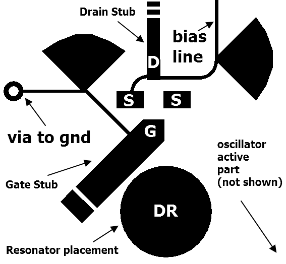
vfone, here is layout of passive part (DR + FET transistor as a varactor):

I did some stub tuning, especially drain stub. Now it works much better, current from drain to ground is less than 0.01mA (10uA) now.
Maybe it is because DRAIN and SOURCE pins being not perfectly grounded at RF. It could be optimized for even lower current, but then oscillation stops. I think it is because "gate stub" line is coupled too tightly to DR.
Ideally FETs source and drain are grounded using vias to ground plane, and then negative bias is applied to gate. I am trying to avoid negative voltage circuity, so using quarterwave stub instead.
biff44, about using voltage source, maybe it will work, but there is another problem: when I decrease series resistor value on a biasing line (default is 1kOhm), then I get more and more huge spikes on biasing waveform. I think it is because waveform changes voltage rapidly, so current starts to flow somewhere between FET and bias voltage source.
My further idea is to reduce "varactor" line coupling to DR, and make better RF grounding on drain using radial stub.
Should I ground source using quarterwave stub also?
Varactor to DR coupling is the prerequisite of having a tuning effect. AC voltage across the varactor will increase with coupling and also the DC current caused by rectified AC voltage. Just normal operation.
You can of course reduce the varactor coupling, but didn't you complain about reduced modulation in the first post?
I will try to add a little distance, around 0.3mm. I want get rid of DC because it gives spikes/ringing to my modulating waveform. Filtering makes transition too slow (FSK modulation)
Using a FET instead of a varactor is not so good idea due to Gate leakage current. When oscillator starts to oscillate, the voltage across the tank circuit ( MS Line, DR and Varactor ) increases higher than supply voltage. This tension is not purely sinewave
and it's absolutely got a mean value rather than 0.This is added onto tuning voltage returns into leakage current due the natural behavior of FETs.A kind of "autobiasing" like in A-AB class Power Amplifiers.
voltage coupled Unwanted 相关文章:
- Induced voltages on transmission line by plane wave in HFSS
- Klystron output voltage, cavity field strength
- Negative voltage needed in K-band
- How to set the bias voltage of the BJT in Gilbert mixer
- is DC voltage gain not an important issue to consider in LNA designing?
- Power (Voltage / Current) inducted in rectangle antenna.
