S-parameters and total loss, calculation approach
we have three cascaded RF components on an our transmitter and we want to calculate the total loss, taking into account the insertion loss of each components, insertion loss of the microstrips used for the layout and the mismatch loss between a component and the other one.
We have the de-embedded S-parameters of the three components obtained from the manufactures, and S-paramters of all microstrips that link them, derived by electromagnetic simulations.
We know that we can convert the S-paramters into T-parameters and calculate the total loss by multipling the individual matrixes with each other. But we are not very sure of result, because of the fact that the S-paramters of components are de-embedded while we have placed the excitation ports for the microstrips under the input and output PADs of the components in order to have the S-parameters of the microstrips.
May you help me to understand if the calculation approach is right?
Many thanks.
Best regards,
Antonio
Hi Antonio,
the basic idea is fine, but the devil is in the detail here.
While working in EM support, I have seen many mistaked related to port placement, port ground reference, port calibration in simulation and reference planes in measurement. Your concerns are very valid. You should provide a bit more detail how you EM modelled the ports, and what/how you de-embedded for components, and also include some screenshots.
Best regards
Volker
Hell Volker,
thank you for reply.
I'll try to describe a bit better the issue.
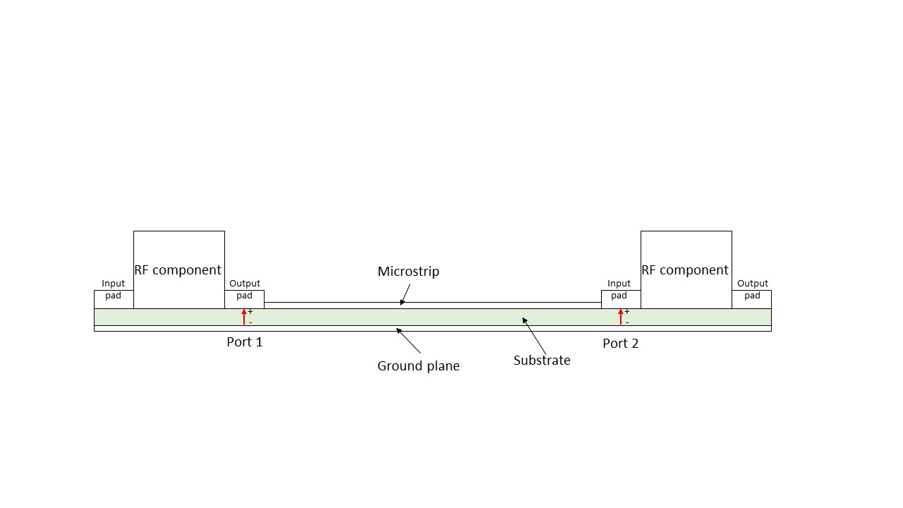
The board has a reference ground plane under the RF lines. Each line links the output pin of a component with the input pin of the next one in the chain.
I have simply placed a lumped port that has the positive on the input/output PAD of the component and the negative on the ground plane. The negative is chosen as close as possibile to the positive. By this way the port appears vertical in the 3D model, as shown in the attachment figure.

By simulator, I have obtained the S-parameters of the only microstrips while the S-parameters of the components are already avaiable and provided from the manufactur. I have no idea on how they have been measured. I am supposing they have been de-embedded up to the input/output pin of the component.
Best regards,
Antonio
That's fine. If your line at the component is really wide, then the type of feed might matter (current from port at one point vs. current excitation over the width of the line), as documented here: http://muehlhaus.com/support/ads-app...edge-area-pins
Reference plane at component edge is a reasonable assumption. There is some uncertainty how much pad capacitance and pad length/phase is already included in the measured data. If you include the pads in EM, you might have too much pad capactance (pad included in both EM and component model) but if you leave them out you might have too little (pad not included in component model and not included in EM model). Also the capacitance from component body to the PCB ground will vary, depending on the substrate material and thickness. Some component libraries describe that detail in documentation, others don't.
Regarding the PCB EM model, you might want to including coupling within the layout, and then end up with a multiport S-parameter dataset. It's not clear from your post if you do that already, or simulate the line segments individually.
The lines are 0,26 mm width.
The EM model contains the pads of the components, but actualy I do not know if this is taken into account also in the S-parameters of the components. I have made an assumption regarding the fact the S-parameters are de-embedded or not. In addition, I have not modelled the component in the EM model, but only its footprint, i.e. the pads.
I have simulated the lines individually. I didn't take into account the coupling among the lines. Might it be necessary to consider the coupling in your opinion? We are working at 500 MHz.
Thank you.
Best regards,
Antonio
Hello Anton,
Regarding your inquiry, you have 3 RF devices with their embedded s-parameters and described ports in a correct-way(meaning the E and H fields are flowing as would expected in 3D EM views)
An approach which works for me is to model the circuit in a hiearchical way with s-parameters.
An example would be, lets say u have W=1mm for 50ohm line impedance,
1- put your N-port device with the manufacturer's S-parameters,
2- put two tapered lines of say 0.5mm to 1mm in some length next to the device(modelling the pads of the device which is usually thinner than the TLine itself).
3- place Tlines and your SMT or distributed components(matching circuitry) side by side in the simulation.
4- Make s-parameter simulation of that circuit, and save its data(This is 1 of the 3 cascaded elements)
Define a new Nport device(with all the matching circuits inside) from input to output, and take it's S-parameters(with the chip's s-parameters buried inside) as your block's parameters.
If you do this for all 3 of your devices, you should have 3 s-parameter files for 3 boxes. Then you can make a simulation with those 3 boxes, and it should give what you want?
Ok, then no problem.
Sure.
It always depends on the circuit function what level of coupling matters, but from what you described, simulating the lines individually should be ok.
total loss calculation 相关文章:
- In distributed amplifiers, is it total input capacitance of the gain stage or Cgs
- Calculating total radiated power (TRP)
- Insertion loss reduction for matching networks in PA design
- Issues with measuring return loss
- Questions about S22 calculation of frequency tripler in ads simulation
- MC145151/2 p2 calculation dip swich vs xtal divader
