Generating the waveform as in the image
1) buy a signal generator with burst function.
2) use a dds chip
3) use an fpga with a DAC and create your own dds.
4) use a 3KHz oscillator and a fet switch to gate a 27MHz oscillator.
5) etc., etc.
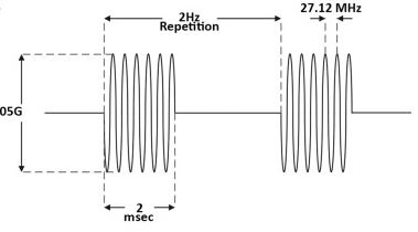
your drawing shows the 27 MHz blast starting at 0 and falling
and ending at 0 and falling
how important is that?
a 2 ms burst is 54240 cycles of 27.12 MHz
how important is that?
what is the peak voltage of your sin wave?
is the signal +/- relative to ground, or is the low (trough) side ground?
Use the FY6600 generator and connect the first source to the second generator, first square wave with 2 Hz period, 50 % duty cycle, and the second on/off modulated and carrierfrequency of 27 MHz
Hi,
Why 50%?
I'd rather expect 0.4%.
Klaus
Yes bro i am trying the third option i am using 27MHZ crystal oscillator which is giving a sine wave having a frequency of 27 MHZ but dont know how to switch the signal on and offf?
Hi,
Just go the usual way: use a switch.
There are "analog switches" that can be controlled with logic levels signals from an FPGA.
Klaus