Could anyone please help me confirm the Simulation results of ADS2016?
I want to use ADS2016 from Keysight to Co-Simulate the PCB layout with RLC.
But for the first step, I found the layout simulation results were not believable.
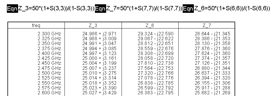
The real part of the impedance of the pad directly connected to the GND plane seems to be too large,
is about 27.8Ω @f=2.45GHz. And the imaginary part of the impedance of the pad directly connected to the GND plane is minus.
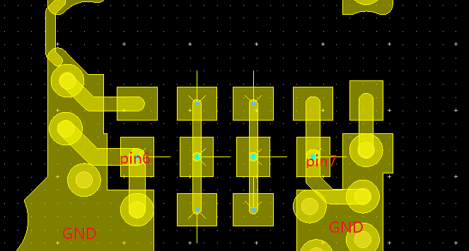
The layout and pins are shown in Fig.1, the pins are automatically added when I converted the PCB file to the ADS files,
and pin type is the none calibration type.
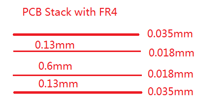
The PCB stack is shown in Fig.2, all PCB material parameters have been set in the simulation file.
The simulation results are shown in Fig.3.
Please refer to the attachment for the archived workspace files of ADS2016.
To let you help me check the files as conveniently as possible, I also archived the simulated dataset in attachment.
Could you please help me check whether there are some mistakes in my simulation or give me some
explanation why the real part of the impedance of the pad directly connected to the GND plane is so large,
and the imaginary part of the impedance of the pad directly connected to the GND plane is minus?
Thank you very much in advance!
Joshua

Fig.1

Fig.2

Fig.3
I looked at your files briefly. Your testbench requires a separate SMD library, and 3D preview doesn't work without adding that.
Your vias in the Momentum stackup don't exist in layout. There is a layer DRILL_TROUGH in layout, but that is not mapped in the Momentum substrate. So all your pads are floating (ungrounded).
~~~~~~~~~~~~~~~
Amendment after looking again at your model: I missed that your substrate does include the DRILL_TROUGH, but the ground paths are ungrounded for another reason: Momentum doesn't know that your EDGE_BOTTOM is your ground. All your EM ports have the reference at GND = global ground, which is the nearest infinite ground plane, or in your case some abstract ground reference at infinity. So your "ground" polygons are not connected to the port ground reference.
To make your EDGE_BOTTOM act as ground for the EM ports, you need to place explicit ground reference pins, and assign them to the port's minus terminal in the EM port editor.
~~~~~~~~~~~~~~~
Data display: You have several ports on one polygon, and I have some doubts if your math gives the result that you are looking for. For your pad with a total of 3 ports, you get 25 Ohm input impedance, which is 50Ohm || 50 Ohm from the other two ports.
I guess you want to calcuate shunt capacitance? You can use function stoz(S) and stoy(S) in data display to get the Z values (impedance with other ports open) and Y values (admittance with other ports shorted).

Hi,volker@muehlhaus, thank you very much for your response.
Following your valuable suggestion, I got the correct results. The mistakes are made for the port setting in the simulation. Because this is a finite GND, the pin+ should reference to the
explict reference pin-.
Yes, I want to check the via influence to the circuit performance.
For the problem of several ports on one polygon, I haven't check the results. But I should connect several ports on one polygon because I should connect several SMD components
on one polygon.
Hi,volker@muehlhaus, thank you very much again.
Yes, many ports on one polygon is fine, but your data display equation (S33 -> input impedance) was not correct/useful for this situation. This gives pad loaded with all other port impedances attached to the polygon.
Better use stoz() or stoy() instead, as shown in my screenshot.
