Required help in simulation of Ungrounded CPW Structure in HFSS
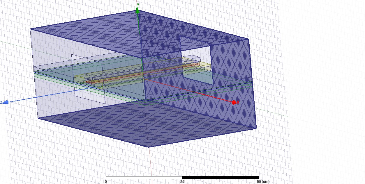
I am simulating an ungrounded CPW structure through HFSS. I used all the references available on edabaord website and followed HFSS tutorial on CPW but still far from getting good results.
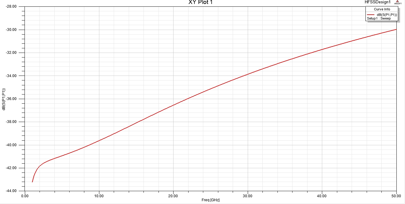
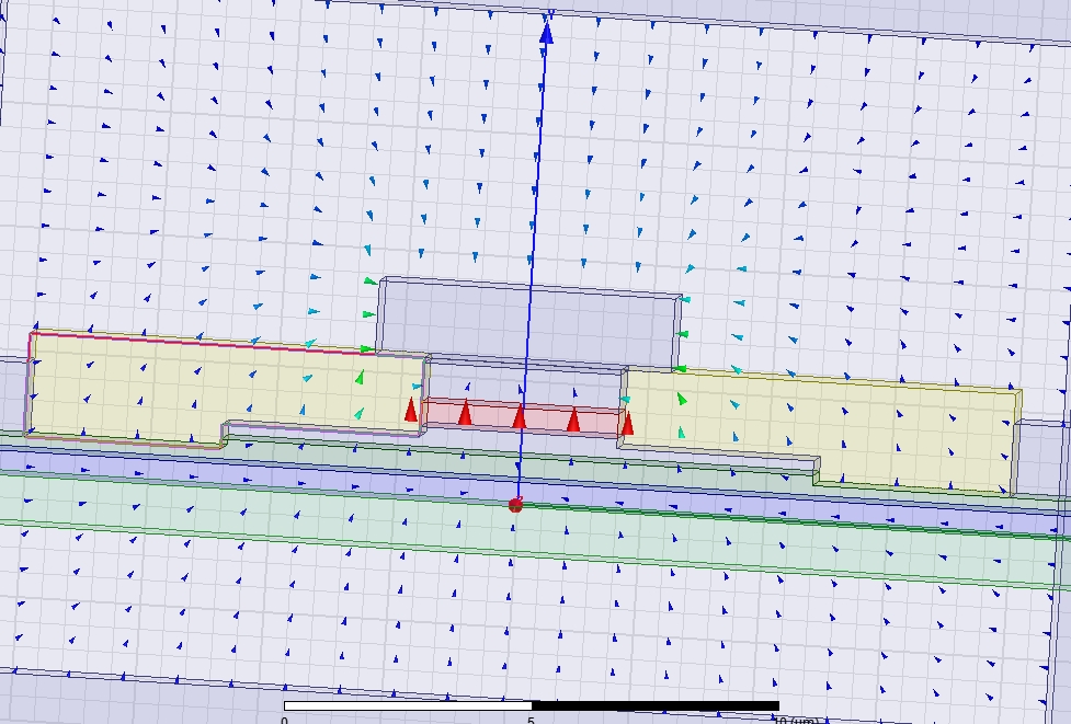
The field profile and s11 curve is shown below. The field is stronger in the intended i-region but its pattern is not satisfactory.
I am also attaching the HFSS file used in the simulation.
I request the edaboard member specially senior and full member to help this Junior member here.
Thanks
Best Wishes
S.Sehrawat
Sorry,
The images are given below.

Hi SudhaSehrawat,
Can you elaborate on the structure you're using, and what field distribution you expect to see?
Dear Sir,
Thanks for the reply.
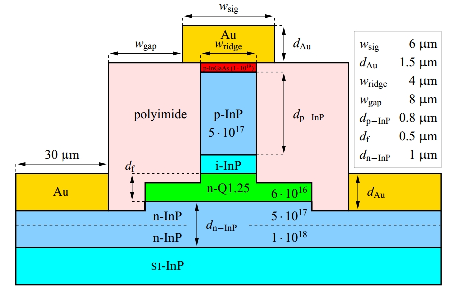
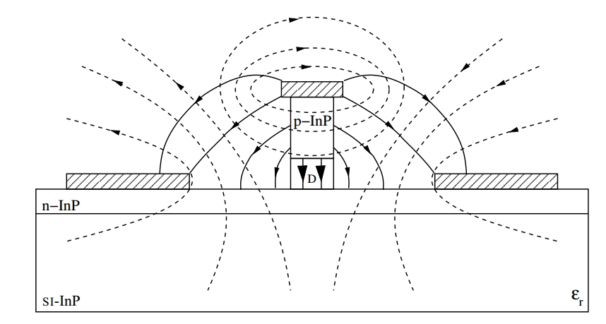
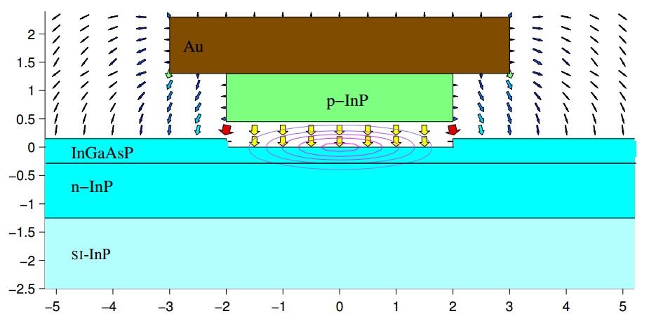
My structure is a pin photodiode whose dimension and expected field output is given below. The field is calculated with other software where width of arrow is proportional to field. The field is expected to be higher in central i-region (i-InP) and should be similar like a CPW structure as shown schematically in third figure.

I have no doubts that a EM solver can calculate the transmission line structure correctly based an thorough material and geometry definition as well as appropriate meshing. Your expectations may be simply wrong.
I don't understand however the exact problem. What's the meaning of the S11 magnitude plot? You didn't yet tell about targeted parameters.
Dear FvM,
I am grateful to your for your prompt reply.
The expected results are already given in previous post. The objective is to have low reflection (s11) at 40Ghz. I just want a second opinion from the professional like you to validate the authenticity of my results.
Therefore, Please have a look on the attached HFSS file and give your valuable suggestion for improvement.
-One Boundry side is not defined ( is there any particular reason ?)
-iInPh materiel is not defined.Check your materiel properties.
iInP and nInPh are defined as per their property please check their moblilities values. Yeah, I m not sure about boundary defined. Actually, I have an example from HFSS library about CPW in which they assign the boundary in the same manner and getting expected results.
You'd want to define all boundaries; I'd guess you'd want the missing one to be a radiation boundary.
Looking at the field distribution and S11, it looks like you're getting what you want. What is your specific concern?
Dear PlanarMetamaterials, Yeah, Its right, I am getting the expected results.
My few concerned are given one by one :
1. If Field goes outward or inward from Signal to ground. Can we say both are the same thing?
2. The S11 parameter is different that one can expect for a CPW line. The conventional cpw S11 plot is shown below :

3. How we can sure that the obtained filed as shown above is only because of single mode excitation and other modes are not disturbing its behavior.
Some of the question can be very easy but I am really confused. I am very happy to receive the quick response from edaboard member and especially grateful to planarmetamaterial.
Yes, the different polarities are just a phase difference.
By exciting a single mode in a driven modal simulation.
Finally, I did that. I was so wrong !
The best way to finish this was to use CST. HFSS is not a good tool for CPW analysis of such structure.