Re: HFSS port 'Port1' does not have a valid reference plane above or below it.

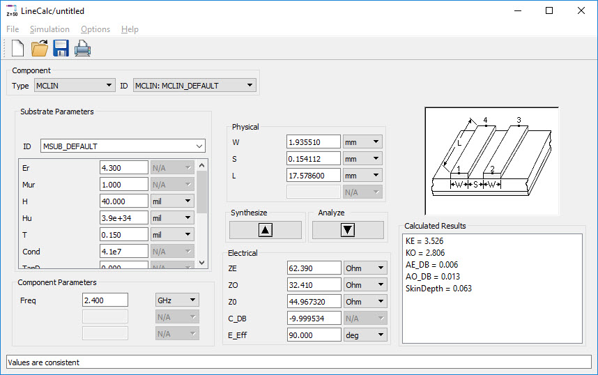
What are you trying to show? Do you think HFSS has different physics? No numbers in your screenshot, so this tells nothing, except that you are using the wrong calculator (one single line instead of two coupled lines with Zoe/Zoo).
EM simulation is only as good as the user's training to the tool. I am working as an RF EM simulation expert for more than 20 years, and was trying to help you here. But it seems to be a waste of time. Good luck!
Sorry, I am not a good user yet.
I have already tried the calculator, but it gave a so small width for a 50 ohm that the smallest via library part could not fit in.
If you want wider lines, for a given line impedance, you can increase the substrate height.
Calculating backwards from the Zoe/Zoo values, it seems that 40mils FR4 was used in the paper.

I have followed all your suggestions, but still it is not behaving like a balun at all
Do you use HFSS ? If yes, I could attach the latest HFSS project files here in this forum.

Again, do not worry too much on the edge boundary in HFSS.
Those virtual boundaries are only for EM simulation purpose.

I understand solver boundaries, but you misunderstood my comment. Two of your feedlines are close to the PCB edge, which is not a good idea because it changes the line impedance (in real life as well as in simulation).

No, I don't use HFSS.
If you are able to export your layout in 2D format (DXF for example), I can check using another trusted EM solver. Exporting the top layer and via is sufficient. I also need to know your PCB materials and dimensions then.
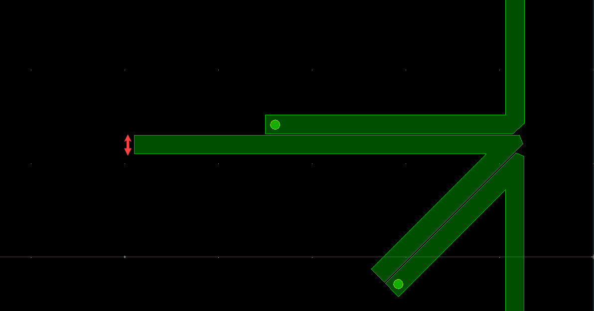
I have attached the dxf file here in this post, but I am not sure if the format fits your own EM simulation software.
planar_marchand_balun.zip
I seem to have a problem with units in your file - please tell me the feed line width, so that I can double check.

Also, there's a bunch of overlapping circles for the via with various dimensions, what is the desired drill (via) diameter?
If you were referring to the width of the red arrow in your dxf screenshot, then it is 2mm as measured inside HFSS
what overlapping circles ?
The paper authors did not state specifically the via diameter.
Note: I am using standard library part for the via. I did not create the via physical shape on my own.

Ok, then I will use that for scaling. It seems I have a mil<>mm issue, which is not unusual for DXF.
There's a bunch of different circles in your file, some are offset from the center. Below is what the DXF data looks like.
Not sure why, and what HFSS does with all that overlapping material definitions.

Here is my model and result when using 40mil FR4 with eps_r=4.3:

The lines inside the conductor indicate the meshing, you can ignore that information. For vias I used 0.5mm diameter.

So, HFSS is quite unusable for layout ?
What tools were you using for layout and simulation ? Is it ADS ?
And in which software program you used in the first two screenshots in your post above ?
I can't comment on HFSS layout capablities, no idea. It might be user mistake, for such tools a week of training is highly recommended. My screenshots are all from ADS.
Ok, I have removed the overlapping circles within HFSS, I found out that I added them accidentally previously and they are not visible as I had told you.
But the question is even after I had removed the overlapping circles (vias) , the layout still does not behave as balun in HFSS simulation.
Then, I tried to import the DXF into ADS, but I do not know how you got around the following ADS error during simulation
I have uploaded the latest, unmodified planar_marchand_balun.zip dxf file freshly exported from HFSS.
As the message says, you need to define units and resolution.
Options>Technology>Technology Setup
Use the standard settings work layout work in millimeters: units mm, database resolution 10000
Not sure how you created you workspace, usually there is a dialog upfront that asks for your choice (mm oder units).
I attached my workspace, layout is your initial DXF.
marchand_wrk.zip
I was having wrong simulation result in HFSS.
So, I am trying with ADS instead for now.
I have problem with EM simulation port setup as shown below
Clicking any button in this dialog does not do anything, I mean it just stay whatever it is. And I cannot add port both manually or automatically.
Why ?

Edit :
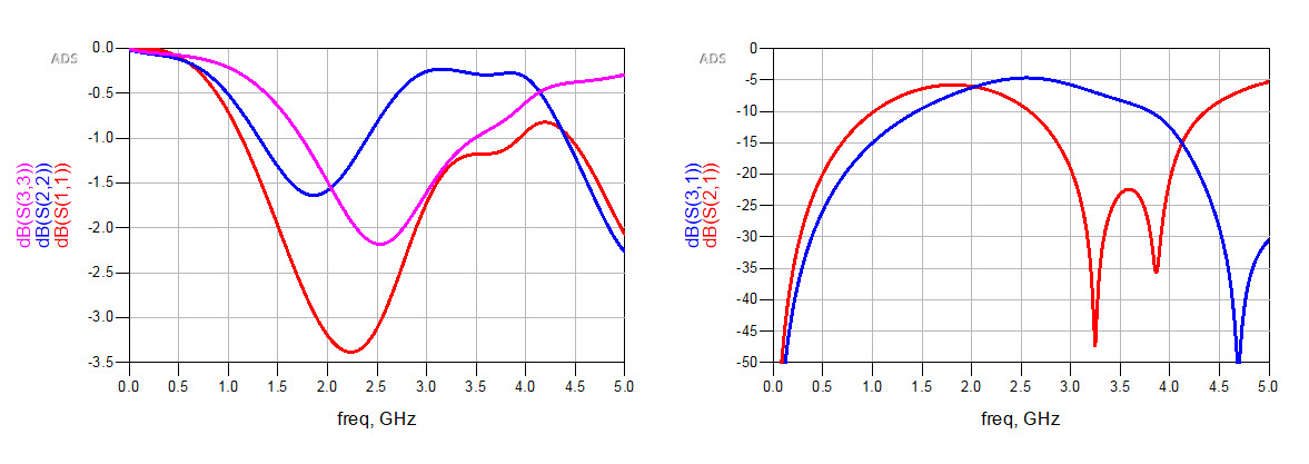
Do you interpret the following HFSS phase plot as correct balun simulation result ?

Pins must be placed in the ADS layout editor, the port editor is then used to assign layout pins to simulation ports. Background: In some cases, EM ports might consists of multiple pins, for example in coplanar with plus and minus pins.
Sorry I can't do ADS Momentum crash course in a few forum posts. My EM trainings on site take multiple days. Keysight offer excellent trainings for layout editor basics + Momentum (3 days to 5 days).
Here is the S21 and S31 phase for the initial DXF. Not 180° difference exactly, but in your layout the coupling segments lengths are different anyway.

Ok, I understand. May I ask a few more questions ?
Sure, I'll try to answer. Maybe you can start from the ADS workspace that I uploaded - that one is complete and you can have a look at my configuration.
The problem is that I just found out that I do not have access to ADS software now.
I do not know why the dxf file extracted from HFSS to ADS simulates well for you within ADS, but not within HFSS.
Now, let me see if I could get the same layout simulates well in SonnetLite.
Sonnet Lite is too limited to simulate this model with the narrow diagonal gap.
Don't blame the tool. From more than 20 years in EM simulation: there is a lot of possible user mistakes. New users in EM always underestimate the importance of learning the tool. Maybe HFSS support can review your model.
- Exporting HFSS design model to GDSII file.
- How to check recevied power in the HFSS port?
- Importing data from HFSS and ploting in matlab
- Defining Lumped port in 3D spiral coil for different values of sweep in HFSS
- HSS Port refinement Error
- Adding/Importing PCB enclosure(step/iges file) to HFSS 3D layout
