ADS co-simulation taking too long
1)designed the tapered line and the 50 ohm one in a layout and did the same thing in another layout for the second pair of tapered line-50 ohms line.
2) i created a variable Ltaper and Lline for the first pair and at the layout design using subnetwork type and placed these variables at the default values of the tapered line and the mline. I did the same thing at the second layout for my other pair and named the variables Ltaper2, Lline2.
3)after defining these parameters i defined the frequency band, the substrate i'm using the mesh size created the EM setup for simulation and placed the necessary pins at the points wich i want to connect the components to the schematic.
4) i created a layout-lookalike component for both of my layouts
5)In the schematic i placed both components using the component library.
6)I placed 4 vars on the schematic (two for my tapers and two for my mlines), made them optimizable(put a large interval for my optimization values) and assigned these variables to the values of the variables of my components(just like an ordinary optimization process in ADS).
7)placed an optimization controller set the goals for the optim and run the optimization
But the thing is that the optimization process just takes impractical time to complete, for instance i let the computer all night and just completed two iterations of the 400 i set and i don't know if something from what i did is wrong. Does anyone know if i did something wrong in this process or why does this takes so much time?
It doesn't seem that you checked what topology and parameter range can provide mathing, and instead just tried "something" with range "almost anything" as a brute force approach. Not so great. Have you checked that a taper can - in theory - do the required matching?
The band of interest is pretty large because it's {27-33}[GHz] and i have seen some other people that did something very similar to what i'm doing and they used tapered lines followed by 50 ohm lines to match these s parameters that correspond to an impedance value lower than 50 ohms. So because i would like to go from a 50 ohm line to a cavity wich has a much lower impedance i used tapered lines as i have seen it from others that did the same. At first, i did the matching in the schematic and from what i saw at the end of the opt when the S11 and S22 goals were met, the lengths of tapered lines and 50 ohm lines were near the highest optimization value wich was 400[mm]. But when i tried the same thing using layout components instead of schematic models the optimization would run forever without progress
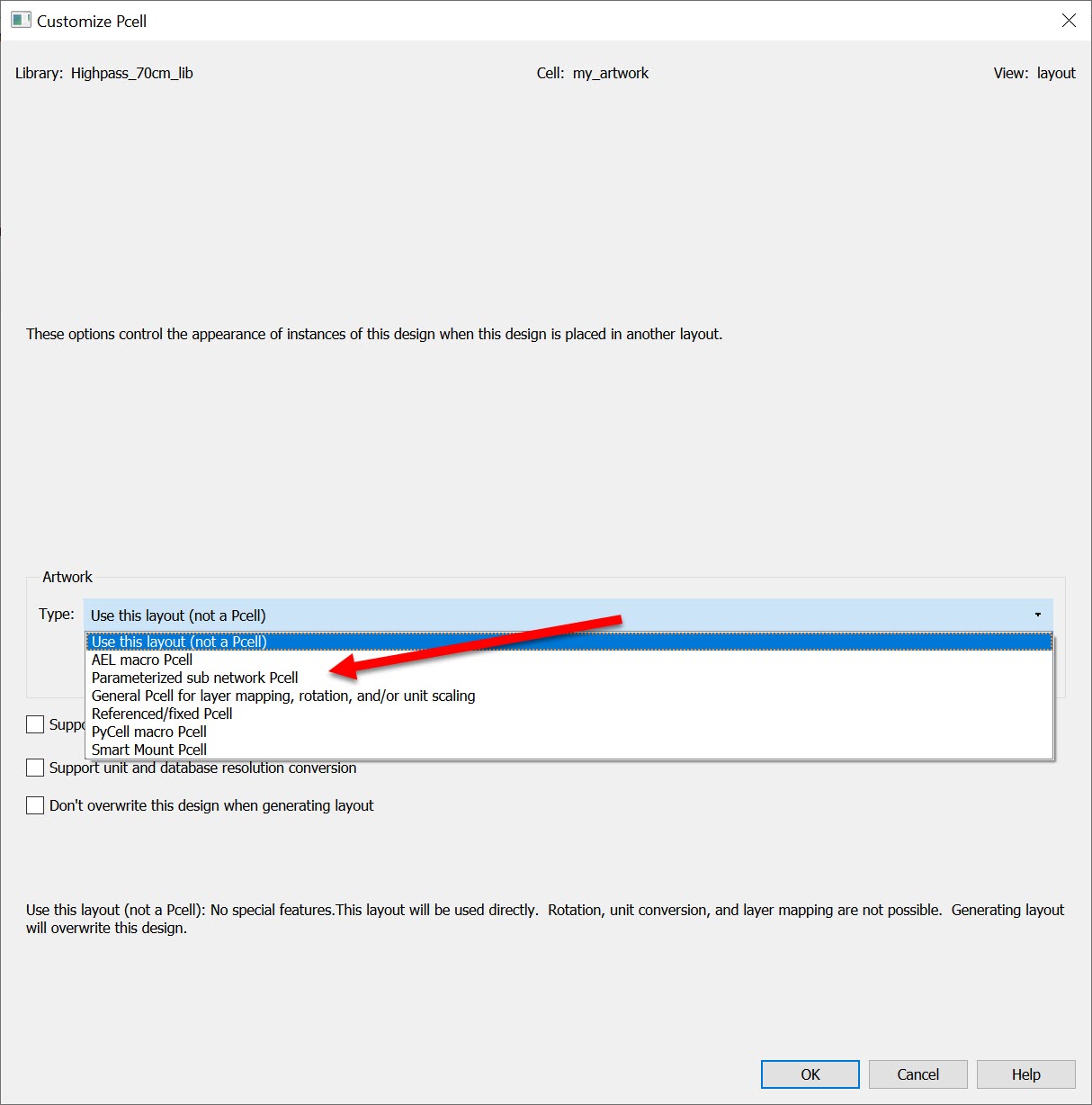
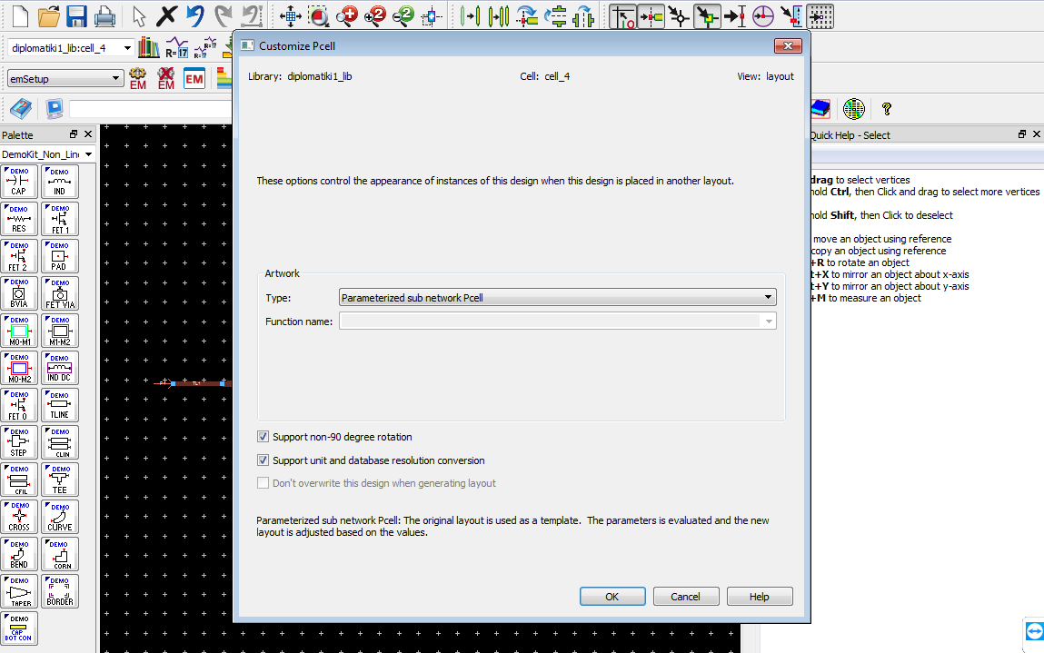
If you create a parameterized layout cell, there is one possible user mistake: By default, the cell layout is fixed ("Use this layout") and doesn't change. See my appnote on parameterized EM: https://muehlhaus.com/support/ads-ap...eters-momentum
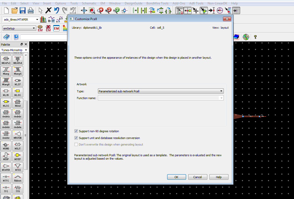
In ADS2020, this is set using "Customize PCell"
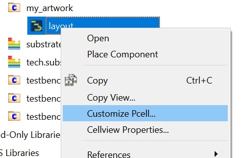
You want to have "Parameterized sub network Pcell" so that parameter changes are passed to the cell and layout is updated
I recommend to set up a parameter sweep first, and make sure your cell does change as expected. Another test is to place instances of your parameterized layout cell into another layout, and see if that changes when you change parameter values.
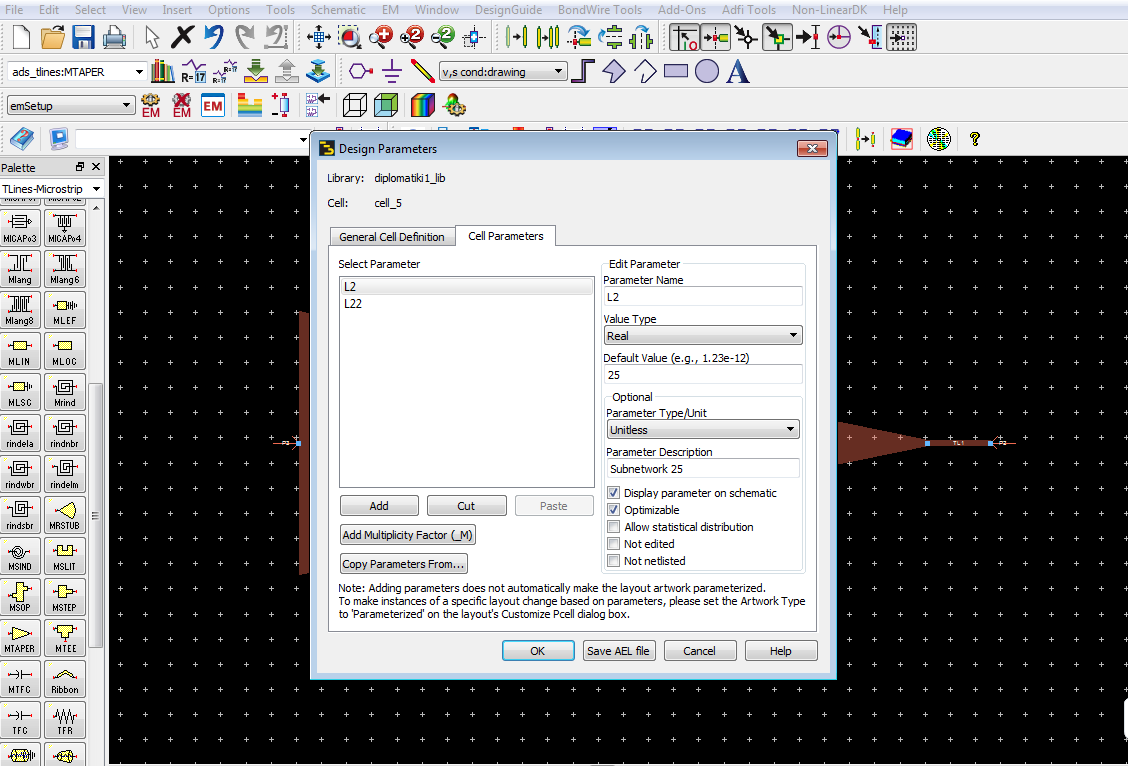
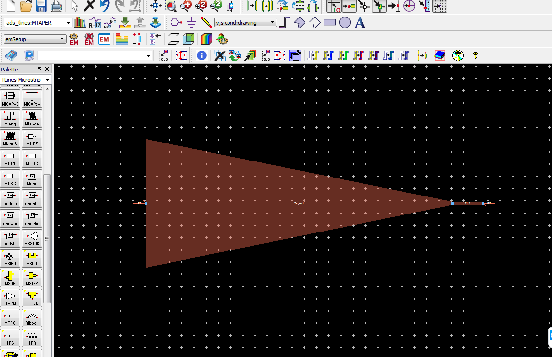
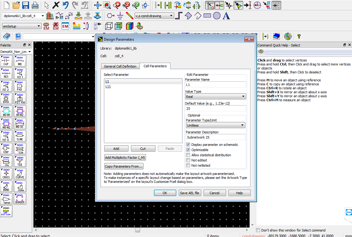
okay i tried parameter sweep for both of my istances but when i saw my template layouts there wasnt any change but i guess the template layout should'nt change but when i'm running the sim ads doesn't create two layouts in wich there will be my two components modified depending on the component's parameters i'm choosing each time. But when i check both em modesl for b i see that after every sim when i had changed the parameter values the new parameter values are actually stored at each em model. I have parametrized both layouts and created my layout parameters there wich defined as subnetwork parameters placed pins at the begining and the end of each component. I have also attached some images of my schematic and layouts. So i don't know why my layout shape stays fixed and at the same time the new values are stored inside the em model without modifying my layouts. The two em models correspond to two different layouts(first instance: X1 second instance: X2)
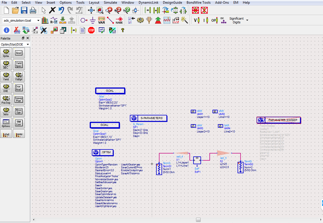
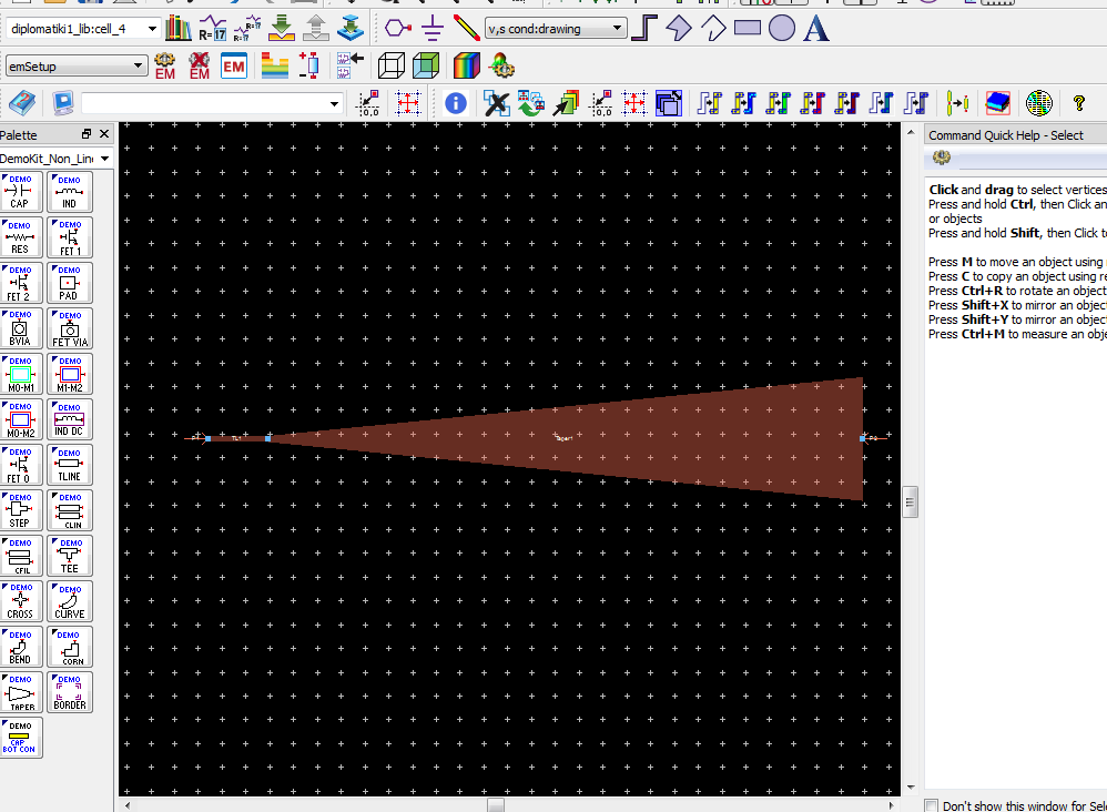
Having multiple entries in the emModel doesn't mean that the layout has actually changed. The ultimate test is what I wrote above: place two instances of your parameterized layout cell into another layout, with different parameter values, and and see if parameter changes have an effect on layout.
If you want to upload your workspace, create an archived project and upload it here. But switch EM data OFF when archiving, otherwise the file is too large.
sorry for my late response as i was off for a few days. i placed my two components and tried some different values and before that i placed the two instances in a layout. I saw that every time when i changed values from schem when i closed and repopened the layout the components were modified accordingly. I have also attached my workspace here.
Ok, the cells scale properly.
Similation method: Your random optimization approach looks inefficient to me.
I didn't try the actual simulation because I don't have that demokit installed (complains missing when loading workspace).
Accuracy: I have some doubts regarding 5mm wide ports at 30GHz, because ports must be small compared to wavelength. That's not an ADS issue, it is physics because wide ports can be overmoded. Your ports are set to use TML calibration, but that requires single mode propagation. I wouldn't trust those results - not until the port width is defined properly.

If the actual device at the end of the taper has less width than the taper, see my appnote here how to control the port width:
https://muehlhaus.com/support/ads-ap...edge-area-pins
As an alternative, you can insert a very short length of line with the actual device width.
If the device/terminal width at that "wide end" port is > lambda/10, you have a design issue anyway.
As for the port widths i chose the widths to be that wide because my structure(wich is simulated in another EM simulator) has port with these widths and i wanted the tapered lines to match exactly with these ports, that's why they are big. Of course, i was concerned about the ads warning about the pin size but i didn't modified it because that was the widths i was supposed to give. As for the optimization method the concept is to match the impedance of a wide port to 50 ohms wich is the impedance of the mline that will carry my signal from the source to my structure and i followed others who chose linear tapers to do it so i thought that to optimize the design i would have to optimize the lengths of these four microstrip lines. I didn't think of any other optimization concept. I re-attached my workspace with the demo kit inside. Also, should i change the calibration of my ports?
The S2P file is missing.
I don't think that random optimization with 4 variables is efficient for EM-based simulations. Have you tried to find a mathcing solution using circuit model taper first, so that you know what parameter values are expected?
Not sure about the wide port. The EM currents looks ok (no other obvious modes), but in general it is not valid to cut such structures into pieces when multiple modes can propagate. I would double check results very carefully using a full (undivided) simulation later.
I also did the optimization process using only circuit components for the mlines and the tapers and got very close to my S11 and S22 goals(less than -10dB for the whole spectrum i'm using) saved the values that came from the optimization and simulated again the circuit to check my S21 and S12 parameters. But when i plotted these i saw that they were worse than before(when there wasn't the maching circuit), that is, my reflection coefficients got smaller but also my transmission coefficients deteriorated but they should become better instead. And when i try bigger lengths for my tapers and mlines S11 and S22 become even smaller but S21 and S12 become also smaller and i think this is not physical. I re-attached my workspace when i have my two layout components also my schematic components (i deactivate the circuit models when i use my components and vice versa) and also there are two deactivated terminals wich i use when i want to plot the s parameters from the s2p file as they are(the term impedances for the latter case were chosen as average values of my two port input impedances when i first simulated my structure)
It can be physical if the taper is lossy. One way to check that is to look at |S11|2 + |S21|2 of the tapers. Result is between 1 (for lossless device) and 0 (completely lossy)
Can you tell me a parameter combination that is expected to work? I'll have a look at your data later.
A combination that works efficiently for my S11 and S22 is: Lt1=34.905[mm] (it is the left taper length) , Ll1=14.9008[mm] (left mline length) , Lt2=33.7427[mm] (right taper length) and Ll2=18.0804[mm] (right mline).
As for the widths, w of the mlines is 0.250672[mm] (50 ohms at 30.5 GHz) for the right taper wide side:5.2 [mm] and left taper wide side 10.5[mm]
The taper width is reversed in your model:
left is cell4 with w=5.2
right is cell5 with w=10.5
I looked at internal losses your matching circuit. To do so, I put them back to back and calculate the total power of transmitted + reflected waves. For a lossless circuit, the result is 1 = 0dB. For your matching, the results is around 0.1 which means 10dB losses in the matching circuits when put back to back. This explains why for longer tapers, you get better matching and at the same time less transmission: it's mostly loss in the taper that gives you better S11.
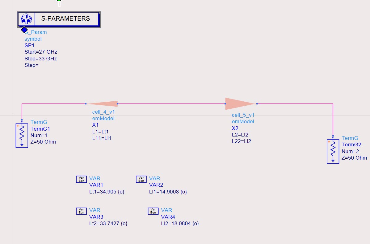
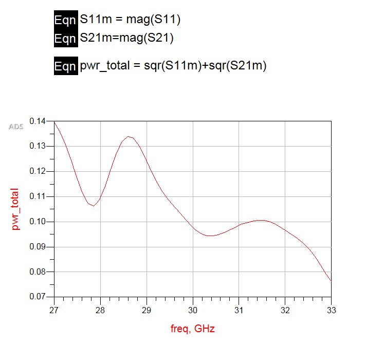
Yes, my mistake they are reversed. So it makes sense now for the deterioration of my transmission coefficients. I guess i have to either use smaller lengths of microstrip lines or try a different matching network
ADS simulation long 相关文章:
