这种运放单位增益响应曲线是否正常?能用不?

相位裕度110度了。大信号响应由于非线性,转换和内部原因出现奇怪振荡曲线,从来没见过这种曲线,不知能用不
通常在考虑建立时间时是不是只考虑达到稳定所用的时间而不管之前的波形?

不能用
bad gain margin
建立时间会很长,PM太大了;小信号稳定肯定没有问题,可你仿真出来的图怎么会振荡呢?
3楼的回答:bad gain margin不明白?求指教
零点太靠里面了
如果我只考虑建立时间一个指标呢?还是不行?波形虽然奇怪,但是后面稳定了啊
不好
为了减小建立时间,需要将相位裕度降低到90以下,才会造成轻微过冲,此时建立是最快的,所以很少会把相位余度提高到110
出现震荡是因为在GBW附近出现了零点,这个零点和附近的极点形成了一条封闭完整的根轨迹,所以会造成震荡
零点消除不太容易,比较容易的办法是将GBW拉到零点之内,我感觉你这个电路需要重新计算设计
关于根轨迹的这句话我没明白。
同样对后几句不是很明白,是零点的位置不是很合适里单位增益出太近了
Your zero and higher order poles (2nd,3rd) are very close to unity gain crossing of Gain plot resulting no gain margin. In simulation you have problem in real chip you will have much worst cases since simulation model accuracy and over PVT etc.
Your input differential pair may have cascodes on them and their Cds creates a forward path to create zeros (or similar situation where parasitic transistor capacitors causing feed forward) and also high parasitic capacitance's in high impedance nodes bringing 2nd and 3rd poles in.
I suggest first to check above and try to minimize parasitic capacitance's (play with transistor W/L), increase branch currents to reduce resistances.If these do not satisfactoryor desired then modify or change your topology.
Good luck!
零和更高的极点(第二,第三)非常接近单位增益交叉增益曲线没有增益裕度。在模拟中,你有问题,在实际芯片中,你将有多少最坏的情况下,由于仿真模型的准确性及以上PVT等
您的输入差分对cascodes对他们和他们的CD创建前进的道路上创造零(或类似的情况下,寄生晶体管电容,使前馈),高寄生电容在高阻抗节点,将第二和第三极英寸
我建议首先要检查,尽量减少寄生电容(玩晶体管W / L),增加支路电流,以减少阻力。如果这些不理想或希望修改或更改您的拓扑结构。
祝你好运!
By the way as jxjxhwxstates, waveform is not strange. Indeed quite typical, for example, for low power (i.e. low branch currents) folded cascode opamp.
If you quickly wantto verify it please increase your branch currents as much as you can (take care of transistor regions)and see the corresponding result
jxjxhwx国家的方式,波形是不奇怪的。确实是相当典型的,例如,低功耗(低支路电流)折叠式共源共栅运算放大器。
如果你很快要验证它,你可以增加您的支路电流(照顾晶体管地区),并看到相应的结果
谢谢你的建议哈,1711064497,further disscussion
我明白了
不见得不能用,首先要看一下是要用在哪些地方。用在不同的地方对运放具体参数要求不同。
是增益裕度不够导致的振荡哈,之后调整了一下好了哈。
Ringing is typical, but I seldom see this kind of ringing waveform in good designs.
If you say it's typical, could you give me some paper which show this kind of waveform ?
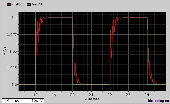
是增益裕度不够造成的哈,在稍大于GBW时相位猛跌至-180度左右而此时增益却突然回升到接近0dB,这造成了时域响应曲线出现振荡
of course, that's why I said it's bad. You must avoid this.
Don't believe in AcoAco. It's definitely not typical.
在稍大于GBW时相位猛跌至-180度左右而此时增益却突然回升到接近0dB,这造成了时域响应曲线出现振荡 ,也就是说相位跌倒180附近时增益没有远远小于0dB,这样就导致增益裕度不够,导致振荡
复习一下奈奎斯特判据。你这种bode plot,根轨迹上会有靠近虚轴的极点存在,所以就ring啦。
这种形状非常不安全,只要你的增益再大一点点,就会开始震荡
Pleaseunderstand that atleast intentionally Ido not advise bad design practices. I did not say ringing is typical for a manufactured product since in first place I avoid a designs with less than 16 degree of phase margin and I try to do anything possible to eliminate bumps close to gain plot unity gain crossings. In fact I try so hard to make gain plot as straight as possible around unity gain crossing. Therefore I myself had never seen those ringings in my manufactured designs at all (I am not even familiar with ringing. To my luck I have never seen even anun-optimal transient behavior) .What we are talking here is a persons attempt to design an op-amp and during the initial phase of his/her design seeing ringings in the simulations ( At least it is what I understood since there is no mention nor photos of a ringing taken on a scope). 
What is typical is bode diagram with almost zero gain margin during initial design phase as shown on the bode gain plot (as I described it typically occurs with very low power designs due to high parasitic capacitance's and high node impedance'sand I tried to give a few hints to fix that. After fix is done there would be at least 15 degree phase margin and no ringing.
Ideally bode gain plot should be a straight line with no nearby bump up (at least minimally a decade away but farther away the better as long as design constraints/budget allows it)after passing the unity gain frequency (i.e. all high order poles and zeros ideally positioned at least a decade away of unity gain crossing, better if farther away)but this requires some design effort with today's very low power designs because high R and C at the nodes and requires some compromises.
I hope this clarify the misunderstanding.
请您理解,至少我不建议故意糟糕的设计手法。
我并没有说振铃是典型的生产的产品摆在首位,因为我用不到一个16度的相位裕度,避免设计中,我尝试做任何可能获得口岸消除颠簸接近单位增益曲线。事实上,我着急使增益曲线尽可能地直,左右交叉的单位增益。阻尼振荡,因此我从来没有见过那些在我的设计制造(我什至不熟悉的铃声。我的运气,我从来没有见过,甚至一个非最佳的瞬态行为)。我们这里所说的是一个人试图设计一个运算放大器和他/她设计的阻尼振荡在初始阶段在模拟中看到的(至少我的理解是正常的,因为那里是没有提及的振铃拍摄的照片一个范围内)。
什么是典型的兆头图几乎为零增益余量在最初的设计阶段,如在波特增益情节(如我所描述它通常OCCURS非常低的功率设计由于高寄生电容的和高的节点阻抗的和我试图得到一些所示提示来解决这个问题。修复程序后,将至少有15度的相位裕度和无振铃。
理想的情况下获得波德图上应该没有附近的凹凸了(至少10年之遥的直线,但距离越远的更好的微创只要作为设计的限制/预算允许它)的统一增益频率合格后(即所有高为了极点和零点理想的位置的单位增益交叉至少十年的路程,更好,更远),但是这需要一些努力,今天的低功耗设计,节点设计,因为它的高R和C,需要一些妥协。
我希望澄清误解。
AcoAco,are you a foreigner? If not, no intention to offend,why is your translation from English to Chinese so weird?
I realize many posts are pure Chinese and majority of forum people do not know English. I do not know Chinese, but I want to help, so I use Google to translate for those people who do not know English (Particularly to reply the ones who ask in Chinese). I also use Google to translate Chinese and translation is indeed funny but through some brain work I understand what translated context is meant.This method works so far with this forum though, since pop up windows contents are not translated by Google, I could not figure out how to attach files and do similar activities so I only write if I could give a useful good answer to othersrequests.
Could u pls recommend some analog design forums ?
I guess it is not allowed to post other forum names (normally all the forums prohibit such activity). I do not want to get into trouble with forum management. I am sorry.
what's your nationanity? are you a student ? I think you are a warm-hearted person,if necessary,we can have a further disscussion through communication tool such as QQ or MSN
高人,人家都没说结构
all of you aregreat analogic IC designers . i hope you can share some typicalcircuitstructures or other proplems we alwayshave todeal. especiallygreen IC designers, just like me .thank you !
that is really a pleasure to communicate with a foreign designer here, and thanks for your help……by the way,I don't know much about the relationship between the "gain margin" and the stability of the opamp, could you recommend some references about that? thank you~
我对外国人接触得不多(都是培训或研讨会场合,我从未出过国),他们,欧洲人,美国人,日本人,韩国人,给我的印象是有修养,懂礼貌,不摆架子,敬业,专业知识强,尤其日本人,特别谦恭。然而在几个外国技术论坛上,我看到的情况是,就专业技术而言,平均水平很一般,不比我们强很多,所以整体来说外国人和我们一样,有牛人,也有垃圾,呈正态分布。当我看到某公司某些人无论什么事,芝麻绿豆的事就打越洋电话请教他亲爹,一打就1个多小时,最后心满意足地,屁颠屁颠地回到他的座位时,我就作呕。在这里,我同样看到了某些人!