利用PNP实现3.3V转2.5V的问题
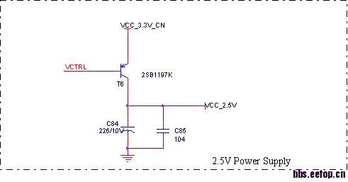
REALTEK公司推荐的2.5V供电原理图如上图所示,其中VCTRL是由百兆PHY芯片给出的控制信号,得到2.5V电源后又给百兆PHY芯片供电。
请问此电路图的原理是什么?此时PNP管工作在什么状态?VCTRL应该给出什么控制电平?(未接PNP时我测得VCTRL是低电平,接上PNP后变为2.6V左右)
VCTRL的电压只要比VCC低一个开启电压管子就处于开启状态。这种接法和让基极和集电极接在一起的工作原理应该基本相同。
工作时候VBE正偏,VBC稍微反偏,PNP管工作在有源区。看着PNP管像个LDO的输出管, VCTRL是输出管的控制电压, 否则怎么保证PNP的集电极刚好是2.5V啊
3.3-0.7=2.6v
这么接应该有一定的保护隔离作用
二楼 & 三楼的看法正確
This PNP is part of the control loop.
Usually a discrete PNP component has a small-signal current gain about 50-150.
It works in active region.
VCTL provides an analog control voltage around 3.3 V - 0.7 V (One Vbe drop from 3.3-V VCC).
In case the loop finds VCC_2.5V too low, VCTL will be driven lower (i.e., more |Vbe|, more Ib), thereby creates more collector current (IC) to charge up VCC_2.5V node, and vice versa.
5楼3楼完全正确,2楼第2句错误
It is usually a single transistor linear regulator, and should have a feedback signal to the controller.
我感觉可以直接降0,7,因为那里有个PN节
今天又做了一个实验,发现如果将集电极开路,则Vc=3.3V 。原理图中的VCC_2.5V给PHY芯片供电,如果将2.5V与PHY芯片断开,另外在2.5V输出上加电阻负载,发现2.5V并不能稳压,变动范围较大。
请问此电路的2.5V稳压性能跟所接负载有关吗?
Yes, the regulator's stability is highly dependent on its load.
I cannot imagine what takes place when the collector of the PNP is disconnected from the power supply pin of the PHY.
My speculation is that the PNP would find its collector current load suddenly disappears (from, for instance, several milli-amperes) to zero,So the collector terminal voltage would jump up to VCC - VCE(saturation) ~= 3.3 V.VCTL would go up only if the regulator loop thinks VCC_2.5V is too high.
On the other hand, if VCC_2.5V already lost its supply source (which once was from the collector of the PNP), how could it be charged too high?
Regarding the reason why simple resistive load would cause instability:
Question: what is the resistance of the resistor you tried?
1 KOhm?
You may want to shunt an additional capacitor with the resistor and try its stability again.You may want to try 1 nF to 10 nF.
I anticipate the on-chip decoupling capacitor has the capacitance in the aforementioned range (between VCC_2.5V to ground).
小编你都开环了,还稳什么压?根据你的图及描述,可以知道基准电压和误差放大在PHY芯片里,2SB1197是外接调整管,集电极c和PHY是不能断开的,你要测负载能力应该直接把电阻并在VCC_2.5V上就可以了
有木有MOSFET实现电平转换的例子呢~
菜鸟求参考,求指导~
想1.2V方波转2.5V