折叠式共源共栅的极点问题
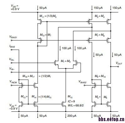
晶体管M5的漏端的RC时间常数在gm/C数量级,但是感觉M5漏端不在信号通路上,所以这个极点不会出现在运放输入输出传输函数中,各位大牛怎么看啊?
不是drain
这个非主极点在M5的gate
the equivalence resistance at the drain of M5 is much, much lower than 1/gm9 because of the feedback loop around M5 and M9. The pole at the drain of M5 located at very, very, very high frequency
你看哈,如果M5漏端电压稍微增加一点,那么M9漏端电压会急剧增加,增加的倍数在(gmro)^2数量级,导致流过M5的电流也急剧增加,这样一来,M5漏端对地等效电阻大约是1/(gm5*gmro*gmro),这个电阻确实非常小。M5的Cgd电容会增加(gmro)^2这么多,而且这个电容是个负电容,那么这一点的时间常数还是gm5/Cgd5,而且是个正极点啊!况且,这一点根本不在信号通路上,应该不会对频率响应构成任何影响啊!在Tradeoffs and Optimization in Analog CMOS Design(论坛上有)这本书中391页,作者并不认为这个地方有极点。一下是截图哈。
还有其他非主极点!
I don't think your analysis is right.
Firstly, why do you think the voltage at the drain of M9 will increase by (gm*ro)^2 times ?
Secondly, why do you think Cgd of M5 will increase the same time ?
Show me the fomulas you used.
我的考虑有点问题哈,频率很高时,M5的Cgs页不能忽略,那个gmro的平方是低频增益,如果考虑高频时,这个增益会大大衰减!这样一来,这个极点很难直观确定啊。而且我感觉这一点确实不在信号通路上,就算极点比较低,那也不会对运放频率响应产生影响啊
M9 source 到 drain 增益是 gm9*Rout
M5 的等效电阻大约是1/gm9(gm5*Rout-1)
非常非常小
你这只是R很小,那你能保证C不变大吗?你怎么算出C?
I do not understand why you think C will increase
大约等于m9的Cgs
我感觉这个电容确实是负的,而且拉扎维有一道题目也与这个电路类似,你看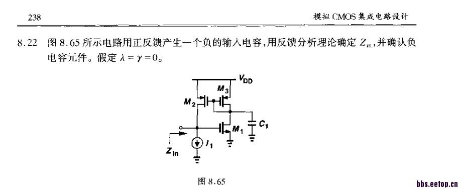
看我的12#帖子哈,感觉有个倍增效应啊
lz
极点是由对地电容产生的
In your circuit, it's negative feedback.
In razavi's circuit, it's positive feedback.
They are totally two different circuit. In which way you think they are similar ?
那你说,如果M5漏端电压升高1mV,由于M5漏端到M9漏端增益很大,假设是100吧,那么M5栅极电压上升100mV,M5漏端电压将会比M5栅极电压低99mV,这样就有电流从M5栅极经过Cgs流到M5漏极了,这不就可以等效为M5漏端的对地负电容嘛,如果是对地正电容,电流流向应该是从M5漏端流向地或者其他地方!我说的哪里有错?
这里的对地电容应该是对地等效电容吧,不一定就是一端接地才叫对地电容
you really think the voltage gain from the drain of M5 to M9 is high ?
you are using "low frequency" brain to analysis "high frequency" signal.
如果M5漏端到M5栅端增益不高,那么这一点阻抗怎么会远远小于1/gm呢,你一开始就说这一点阻抗非常小的哈
那么高频时这一点阻抗怎么可能变得非常小?
because it is a feedback loop. Try to use current way to analize this circuit
难道高频时M9漏端近似等效接地了?这样M5漏端阻抗是1/gm9,不是你说的very very low 吧
什么事current way? 为什么不能用voltage way?
实际上,我认为这一点不会对频率特性有影响并不是认为这一点的RC时间常数有多么小。我感觉这一点个根本不在信号通路上,如果M9l漏端电流增加,无论M5漏端时间常数,电阻,电容是多少,信号根本不会经过这里,信号直接从M9栅极传到M10源端再传到Vout了。你说的current way我是在是不明白哈,不过我们都认为这一点无关紧要。
个人觉得M5漏端的寄生极点还是存在的。M5源端的对地寄生电容会分掉从左边上面下来的小信号电流,使得流过M5的小信号电流减小,进而镜像到M6的信号给衰减了。
至于提到的电容倍增效应,尽管M5的栅端和漏端上的信号是反向的,但不会产生类似密勒效应的效果,M5的漏端小信号电压并不会放大多少,设若M9和M5的跨导相等,M9的源端和M5的栅端小信号电压变化应该差不多,因为两个管子流过相同的小信号电流(暂不考虑寄生电容)。
刚刚手算了下左边端点的对地阻抗(即M5的栅端),确实存在两个极点和一个左半平面零点,没法画图标注,不好给出公式,零点和极点的数量级相当,都是管子的跨导除以寄生电容,具体可以推算下,这样应该还会存在一个极点,也印证原来的想法,由M5漏端寄生电容所引起的信号衰减。有兴趣可以画下小信号图分析下,希望我没算错。
至于负反馈而引起M5漏端阻抗很小,这个需要考虑下。如果M9的栅端是输入端,上面带的是电流源,这样的buffer结构确实有减小阻抗的意思。但folded-cascode的结构,信号是从上面的电流源下来。手算出来并没有看到这个极点在很高频。
希望能对大家有所帮助。睡觉前推算小信号图,有可能会错,希望有人验证下。
Sorry. I made a mistake.
I will explain it much more clearly. I don't calculate it accurately, just explain it intuitively.
Firstly, let us discuss the resistance at drain of M5 at low frequency. If the voltage at drain of M5 increase, the voltage at drain of M9 wil be very high because of high gain which means the voltage at gate of M5 will be high, if take Cgd into account, there will have current flowing from gate of M5 to its drain. it seems that it will show negative resistance. But do not forget the feedback path. High voltage at the gate of M5 also means M5 will drive much more current from the drain of M5. So it's negative or positive ? Seems hard to say. My argument is M5 is an amplifier, but Cgd of M5 cannot amplify signal. So M5 itself will drain much more current than Cgd it self. So We could say the resistance at drain of M5 is very low at low frequency. If calculate it and does not take Cgd into consideration, I think it will show low resistance.
Actually, taking Cgd into account for your circuit analysis will make the problems very complex. So I highly recommend not to take it into account except when you do nanometer circuit design. Just beware of the effect of Cgd when you design your circuit. For hand calculation, it will make the problem very complex.
Then goes to high frequency, That's where I made a huge mistake. The pole at the drain of M5 will not be that high as the loop gain will be low at high frequency. But it still higher than the pole of the drain of M9. The pole of the drain of M5 really exist. You said that the signal will not flow through M5. You are right if you were talking about output signal. But this saying is misleading. Consider there is a signal flow to the drain of M9. You said the signal will not flow through M5. But the real signal we are talking about is the signal flow to the drain of M9. This signal actually will split into two signal. One signal flow to the gate of M5, then this signal will introduce output signal. But there is another signal that flow through M5 and M9 themselves. How large is this signal will influence another signal that flow to the gate of M5. So the pole at the drain of M5 will influence the behavior of the circuit.
电路上的所有零极点都会影响输出,不存在不在信号通路上的点不影响输出这一说
这个帖子扯淡扯的好长啊,实在看不下去了
这个问题其实意义并不大,而且答案很简单
M5 drain肯定有影响,只是被casode M9/M10 relieve了
要想有明确数学关系,自己推公式
其实有个简单的方法,在M5 drain挂 1KF cap,simulation里肯定可以看到
空谈误国啊!......