DAC的问题
建议你打消這個念頭
The reason is the following:
Unit current source 5 uA, mismatch OK (in case you know how to determine the W/L, VGS, etc.) according the mismtach characterizataion report provided by the foundry, and you know how to rung Monte Carlo simulations to verify your design.
Now you change the unit current source from 5 uA to 5 nA.
The mismatch between your current sources (DAC elements) will be deteriorated a lot.(厳重惡化)
(Matching gets worse with smaller bias current).
The INL and DNL of your DAC will become very bad.
If your superviser or teacher asked you to add this option, you may want to convince him that this might not sound like a good idea.The reason is described above.
开玩笑?
那我要做个5nA-5uA的DA怎么办呢
Clarification
Unit current source: 5 nA
Maximum current output: 1023 * 5 nA
Is this part of your design specification?
Can you specify your power supply level (typical and minimum)
The resistive load (on-chip or off-chip) value
Single-ended output or fully differential output ...
1. Do not use wide width device.(for instance,
W_min = 0.24 um,
Width with single contact = 0.42 um,
Width with two contacts is 0.89 um.
Choose width = 0.89 um, and no more wider. <- Choose a MOS device, without significant narrow-width effect, but narrow enough.
2. Choose as long channel length as possible.
3. If possible, use pMOS as the unit-current mirror device, instead nMOS.
The reason is the mobility of pMOS is smaller.With the same bias current, the (VGS - VT) can be effectively larger.
Steps 1-3 are enforced to make maximum VGS - VT possible.
4. Determine Large enough VGS - VT.
5. Employ cascode to increase the output impedance of each unit current mirror.
Example:
Single ended output
Full-scale current output: 1023 * 5 nA ~= 5 uA
R_load = 200 KOhm (full-scale: ~= 5 uA * 200 KOhm ~= 1.0 V)
When all current sources are in parallel, you see r_out / 1,023 of the 1023 unit-current sources.
Make sure this number is much greater than 200 KOhm.
This means your unit-current source needs to have r_out >> 200 MOhm
6. Separate your current mirror units from the decoder circuits.Put all your current mirrors together and make 2-D scramble.This is to minimize the impact of process-dependent gradient.
7. Put at least two columns of dummy current mirrors at the array edge (both sides) to minimize microloadings.
8. Depending on DNL and INL design specification, determine binary weigthted current mirror and thermometer coded current mirror.
寫得比實做容易
你好,谢谢你的细心解答,我一开始是这样做的,电源电压5V,用的是0.35um工艺,单位电流源的尺寸选择w=450nm,l=23.5um。这样可以保证一定的Vgs-Vth,不过我不知道一般要保证多大的Vgs-Vth,还有一个问题我不知道是不是开关电路部分出问题了还是怎么的,输出电路最后有很大的尖脉冲,尖脉冲全部出现在转换过程中。详细的我有仿真图,希望能留下你的邮箱地址,我发邮件给你看也可以
还有一个问题,我实际测试时要用到100K的电阻,还有我做的是差分的双端输出,但实际给下级电路是单端的如何实现呢
看看你运气好不好吧,反正感觉是个很悬乎的东西,5nA,漏电?
什么地方用,需要这么小的功耗啊,
100K load resistor,这个...,noise要多大啊
你的速度要求是什么?
整个方案评估过没有?
在学校里自己瞎整整还可以,反正是烧国家钱
Please refer to equation (11) in the classical paper of JSSC 1989 "Matching Properties of MOS Transistors" by Pelgrom.
You are supposed to get the MOS mismatch characterization report from foundry, which (at least) provides the key mismatch parameters "A_vt" and "A_beta."
Without these parameters, you don't know how much (Vgs - Vth) is sufficient.
A_vt (1-sigma of Vt0 mismatch, assuming W*L = 1 um^2)for 0.35 um CMOS technology is a few mV/um.
(say, 5-7 mV)
A_beta (1-sigma of beta mismatch, assuming W*L = 1 um^2) for 0.35 um CMOS technology is roughly 1.2-1.5%.
From Pelgrom's equation you know in case you set high enough (Vgs - Vth), the contribution of Vth mismatch can be made less.
Then you can calculate the 1-sigma of unit-current source mismtaches based on A_vt, A_beta, (Vgs - Vth), W and L.
Remember you have 1,023 of such unit current devices, and DNL is the worst among these 1,023.
Suppose you want to get yield more than 99%.
Then your choice of (Vgs - Vth), W and L needs to guarantee mismatch causes error < 1 LSB (or even < 0.5 LSB, depending on how you set your design target). ...
Remember, the boundary of thermometer decode and binary-weighted decode is the worst case. ...
Owing to the fact your unit current is so small, my guts feeling says, even at 23.5 um channel length, the (Vgs - Vth) is still not large enough, (but I did not run simulations).
电源电压5V,用的是0.35um工艺,单位电流源的尺寸选择w=450nm,l=23.5um。这样可以保证一定的Vgs-Vth,不过我不知道一般要保证多大的Vgs-Vth,还有一个问题我不知道是不是开关电路部分出问题了还是怎么的,输出电路最后有很大的尖脉冲,尖脉冲全部出现在转换过程中。 ...
No need to check the waveform.
(Since you are using differential architecture,)
Two major factors contribute to glitches:
1. Whether your current sources are always maintained in saturation region (100% of the time),
Assume you have right-side switches, which direct current to the load, and you have left-side switches, which direct current to ground.Your switch driver has to be carefully designed, and delay/load balanced.
(A) The signal delay from clock rising/falling edge to decoder outputs are well balanced.(No matter what code is applied, the delay from clock edge to decoder outputs are almost identical.)
(B) Decoder driver is fine tuned, such that at the time right side switches are turned on (i.e., the current sources start to charge up the load), the left side switches are not completely turned off.Thus there is a short period of time both sides divide the current from the current sources.This scheme guarantees your current sources are 100% of the time maintained in saturation region.
2. How you determine how many bits are thermometer decoded, and how many are binary weighted decoded.
(I hope you are not using 100% binary weighted current sources.)With ideal power and ground, you probably don't observe so huge the effect of factor two from simulation.
Assuming you are using 6-bit thermometer decode (MSB current source arrays), and 4-bit binary weighted (LSB) source sources.
LSB: 1X unit-current
2nd LSB: 2X unit current
3rd LSB: 4X unit current
4th LSB: 8X unit current
The rest 6 MSB's are thermometer decoded, so each MSB current source has 16X unit current, and you have 63 of such MSB current sources.
At first, your DAC input is 00,0000,1111.All you LSB current sources are directed to the output.
None of your MSB surrent sources are selected and directed to the output.
The next time, your DAC input is 00,0001,0000.
None of your LSB current sources are directed to the load, and the 1st thermometer decoded MSB current source is directed to the output.
So the transition from 15 to 16 (decimal), we observe glitch due to switching of current source direction from (non-ideal) ground to the load.
So are the cases fom 31-32, 47-48, 63-64 transtions, and so forth.
If you use fully binary weighted current sources, at 511-512 transition, you observe the largest glitch. (I hope not.)
Your DNL also depends on how you determine # of MSB and # of LSB bits.
Then you to check whether (Vgs - Vth) is large enough to support the DNL you want.
(But this is another topic. ...)
Tip
- Cascode reduces the noise coupling from decoder switching to the gate of current sources.
- You may choose 3.3 V as the power supply level, to complete your 0.35 um 10-bit DAC design.It is an easily achievable target, since you don't not have large output swing.
谢谢你写了那么多,问题是我的工艺是0.35um厚栅的,所以电源电压要5V
然后我现在最头疼的是,如果我输出不接100K的负载,将来测试时岂不是无法测到信号,但是如果接了100K的电阻就会导致转换过程变慢,整个转换周期信号缓慢下降且无法进行一个LSB转换,另外如果使用了50的电阻转换过程正常了,但是就是在转换过程中出现相当大的毛刺脉冲,感觉问题就是出在开关电路部分,可是开关对我来说就是用了一个CMOS传输门,这点我现在仍然困扰着无法解决
不敢说5nA,但是10nA应该能够做得出来,因为我就做了一个
有10nA也行呀,能留个QQ,MSN 或邮箱什么的吗?或者方便的话给些资料也行,我就是搞不定呀,万分感谢了,我最近被老板逼死了
简单说下,输入5.12uA,分两级,通过不同开关控制的电流镜并联产生输出,第一级最小单位电流320nA,用运放控制电流镜两边的漏电压,这样精确,第二级320nA输入,最小10nA输出,然后第一级和第二级并到一起产生10nA精度的电流,注意电流镜的L越大越好,我的是3u,layout注意match。
Q: Did you check whether your current sources are always in saturation (with 100K load)?Do you have "left-side" switches and "right-side" switches?
Q: Why didn't you consider nMOS switch?
再看一次:
1. Whether your current sources are always maintained in saturation region (100% of the time),
Assume you have right-side switches, which direct current to the load, and you have left-side switches, which direct current to ground.Your switch driver has to be carefully designed, and delay/load balanced.
(A) The signal delay from clock rising/falling edge to switch decoder outputs are well balanced.(No matter what code is applied, the delay from clock edge to decoder outputs are almost identical.)
(B) Switch decoder driver is fine tuned, such that at the time right side switches are turned on (i.e., the current sources start to charge up the load), the left side switches are not completely turned off.Thus there is a short period of time both sides divide the current from the current sources.This scheme guarantees your current sources are 100% of the time maintained in saturation region.
If you use nMOS switches, you only have to make strong-P-weak-N switch driver to achieve (B).
还是不太懂,希望可以给个联系方式详细咨询下,或者给个电路图什么的,我是初学者,老板就交给这种任务,我还找不到什么资料,所以希望大大可以不吝赐教。
我呢就比较简单的采用一个偏置电路产生两个偏置电压给共源共栅电流源提供栅极电压,然后数字部分就是分段译码电路,最后经锁存器产生控制信号给开关,控制电流源导通,然后开关采用的是CMOS传输门,但是现在总是产生很大毛刺,这是我的基本情况,能否教教我呢,谢谢啦
还有就是,你的两级变换是在做单位电流源的地方加入,还是做好一个5.12uA单位电流的DAC然后在输出端进行两级变换得到10nA单位电流的DAC,总之,希望能够进一步与你沟通
上一张简单示意图,左边电流输入,中间电流第一级输出,右面作为第二级输入,两级结构一样。运放保证两端输入电压相等,电流能够精确镜像,80dB增益足够了。注意,开关的尺寸也要成比例。还有,我这个原理上是IDAC,但不作为DAC来用,电流的毛刺肯定有,在我这里是没有关系,所以对于你的设计仅供参考。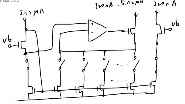
基本了解,可是对于下面这么多开关的作用不是很了解。我的意思是能不能把你的电路给我看看,可以不给参数,就给个电路图,或者你是参考哪个资料的告诉我也行。
还有就是如果我把你这个思路用在我的输出级可以吗?即我先做一个5uA-5mA的DAC,然后用你这个结构产生5nA-5uA的电流。
最后就是我的毛刺实在太大,5nA的电流毛刺就有3uA
谢谢
你好,上次问你DAC的问题,之后就没回应过我,可能过年了,都没上网吧,如果现在有空还能再回答我下吗?谢谢了
你可以使用Current steering + R-2R结构的DAC结构
current source 采用160nA,160nA,160nA,160nA,160nA,160nA,320nA,640nA,1.2uA,2,4uA
在内部电阻上分流(无源器件的matching与电流密度相差不大)
不是很懂,能否说的更细点呢
PS:我要得到的是5nA-5uA的10位DAC
你用这个方案做过了吗?可行否
利用无源器件(多晶电阻)的匹配性与电流密度不相关,对电阻进行折叠,我做过50nA~50uA差分输出10bitDAC
将DAC拆分为4+6结构(或者5+5,具体取决于器件的性能),4bit MSB采用电流源2.4uA,1.2uA,640nA,320nA,剩余6bit LSB全部为320nA的电流源,采用R-2R结构的电阻网络,将6bit LSB分别插入,注意R-2R的电阻的值必须大于实际负载电阻(因为DAC的最终负载为负载电阻并联上R-2R的电阻)
你好,有点知道了,但是可否方便的话给些资料或者框图什么的更形象化一点,我已经加了你的QQ,如果不方便可以QQ交流,万分感谢,我现在急用呀