请教一下razavi第四章一道题
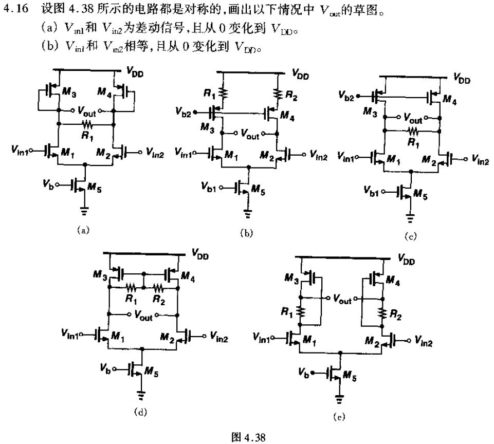
这里面的电阻R1 R2作用是什么?
看不大懂答案的图是怎么画出来的,就第一个看懂了,谢谢指点
In my opinion, the different placement of R1 or R2 set the different output resitance of the differential opam, it can be verified from the different slope ratio in the solution. For example, as for (b), the resistanor act as series feedback to increase the output resistance of the load, so the differential gain is big than others. For (a) and (c), the R1/2 parallel with 1/gm3 or 1/gds3 get different output resistance. Others are similiar.
谢谢指点,但是我还有个疑问为什么(b)、(c)两个的差分输出曲线的转折点和其他的不一样
我是这么算(a)的转折点的:
当M2截止时,Vin2=Vod5+Vthn, Vin1=Vgs1'+Vod5,
delta(Vin)=Vin1-Vin2=Vgs1'-Vthn=Vod1'
而因为M1的电流变为原来的2倍,所以这个过驱动电压为原来的Vod1的sqrt(2)
得到转折点处delta(Vin)=sqrt(2)×(Vgs1-Vthn)
所以有了对b c两图的疑问,盼解答,下图是Razavi的答案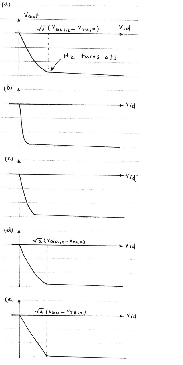
Good question.
For (b) and (c), since the high output resitance causing high differential gain, one of the input device will enter into deep triode region before the maximum input differential input make it turn off, this is why their turn point is smaller than others.
Thanks for your answer!
Before M2 turns off, the device works in saturation region. M1 probably enters tride accounting for the high output impedence.
When M2 turns off, M1 still stays in triode.
This is what u mean. Is it?
You are partly right. Actually, in (b) and (c), due to the high gain, M1 is in deeply triode region after the input differential voltage is bigger the turn point voltage, and we can assume its VDS is near zero, at this time, you can not cut off M2 even if you increase the differential input, that means, the current flowing M1 can not increase any more,and M1 can not sustain all the rail current, M2 will not enter into cut off region.
good!
好强啊!太厉害了!
支持一下
太強了 ~~~
差分信号从0-VDD,应该在较小时可以用直观的小信号分析得出各个电路的差异。但到差分信号增大到一定程度,一个管子高度线性,另一个截止,那就是大信号比较直观了。
个人觉得画出一条转移曲线是综合各种分析方法的简要和准确性得出的,而实际上大信号分析可以解决问题,只是小信号分析时还通过大信号来得到,就显得繁琐了
希望大家多交流
分析的不错