TPS5401问题
设计4V输入,输出3.3V/200mA
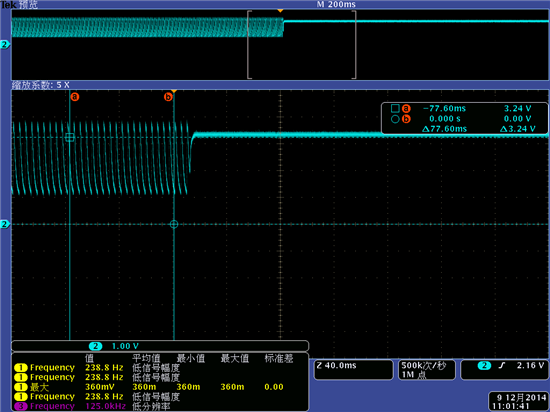
问题:当输入电压降到3.9V以下时,如果频繁插拔电源模块,Vout震荡输出,波形如图。
在输入电压大于4.0时,不会出现上述问题。
补充:当提高输入电压到4.0以上时,输出恢复正常,如下图。
另,输出的震荡波形是否是电源的调整器一直在通、断之间切换?

亲,建议查一下模块输出,是不是输出也成这样了。
你好,你所看到的震荡频率是否跟插拔的频率相同,谢谢。
频率不同,插拔是随机的,没有固定频率。
(1)是否和输入输出的压差有关系
同时用该片输出1.8V和2.5V不会出现该问题,均为4V输入。
(2)输入电压低于3.9V时,极易出现该问题。然后调整输入电压,上升到4.0以上时,能够自行恢复正常输出。
以下来自于datasheet,P13,没有完全看懂这个机制。
8.3.3 Low-Dropout Operation and Bootstrap Voltage (BOOT)
The TPS5401 has an integrated boot regulator, and requires a small ceramic capacitor between the BOOT and
PH pins to provide the gate-drive voltage for the high-side MOSFET. The BOOT capacitor is refreshed when the
high-side MOSFET is off and the low-side diode conducts. The value of this ceramic capacitor should be 0.1 μF.
A ceramic capacitor with an X7R or X5R grade dielectric with a voltage rating of 10 V or higher is recommended
because of the stable characteristics over temperature and voltage.
To improve dropout, the TPS5401 device is designed to operate at 100% duty cycle as long as the BOOT-to-PH
pin voltage is greater than 2.1 V. When the voltage from BOOT to PH drops below 2.1 V, the high-side MOSFET
is turned off using an UVLO circuit, which allows the low-side diode to conduct and refresh the charge on the
BOOT capacitor. Because the supply current sourced from the BOOT capacitor is low, the high-side MOSFET
can remain on for more switching cycles than are required to refresh the capacitor. Therefore, the effective duty
cycle of the switching regulator is high.
The effective duty cycle during dropout of the regulator is mainly influenced by the voltage drops across the
power MOSFET, inductor resistance, low-side diode, and printed circuit board resistance. During operating
conditions in which the input voltage drops and the regulator is operating in continuous conduction mode, the
high-side MOSFET can remain on for 100% of the duty cycle to maintain output regulation, until the BOOT-to-PH
voltage falls below 2.1 V.
Attention must be taken in maximum-duty-cycle applications which experience extended time periods with light
loads or no load. When the voltage across the BOOT capacitor falls below the 2.1-V UVLO threshold, the highside
MOSFET is turned off, but there may not be enough inductor current to pull the PH pin down to recharge the
BOOT capacitor. The high-side MOSFET of the regulator stops switching because the voltage across the BOOT
capacitor is less than 2.1 V. The output capacitor then decays until the difference in the input voltage and output
voltage is greater than 2.1 V, at which point the BOOT UVLO threshold is exceeded, and the device starts
switching again until the desired output voltage is reached. This operating condition persists until the input
voltage and/or the load current increases. It is recommended to adjust the VIN stop voltage greater than the
BOOT UVLO trigger condition at the minimum load of the application using the adjustable VIN UVLO feature with
resistors on the EN pin.
The start and stop voltages for typical 3.3-V and 5-V output applications are shown in Figure 25 and Figure 26.
The voltages are plotted versus load current. The start voltage is defined as the input voltage needed to regulate
the output voltage within 3.5%. The stop voltage is defined as the input voltage at which the output drops by 5%
or stops switching.
During high-duty-cycle conditions, the inductor current ripple increases while the BOOT capacitor is being
recharged, resulting in an increase in ripple voltage on the output. This is due to the recharge time of the boot
capacitor being longer than the typical high-side off time, when switching occurs every cycle.
没明白的你的意思。
当输入电压调整到4.0以上时,电压输出恢复正常。
如下图所示。
你好,这段话的意思是,下管需要关断给上管boot 电容充电,电容电压大于2.1V时开关管不会关断,对于轻载空载情况,电感电流断续,所以大部分时间,PH电压等于输出电压,输入电压比输出电压大2.1V,才能触发上管导通,使输出电压上升。
如果你怀疑是这个原因造成的,可以改变变换器负载情况,看一下实验现象,谢谢。