tps61032电流上不去 求教
使用这个芯片的时候,实测输入电压为3.1V,负载电阻5欧姆,测试出来电压只有4.17V,这个是为什么呢,电感使用的是额定饱和电流10A,4.7uH的。 输出电容选取的220uF的钽电容。这是为什么呢?
空载的时候没有没输出?
空载的时候是有5V输出的
那你仔细检查一下焊接,焊接不好会导致芯片输出不了大电流,特别是底部有焊盘的芯片,要把底部焊好
是否还有其他原因会导致这个问题? 因为焊了2块 都有这个问题 最大到1A输出。 4V输入。 跟电感值有没关系呢?
先空载启动,然后把5欧姆电阻加上,是否能有正常输出?
或者也试试慢慢加大负载
The peak current of the NMOS switch is also sensed to limit the maximum current flowing through the switch and
the inductor. The typical peak current limit is set to 4000 mA. An internal temperature sensor prevents the device
from getting overheated in case of excessive power dissipation.
流过下管的电流会被检测,如果接地不好,检测到的电流信号会有尖峰,会使电流限流误触发,所以查看你的PGND以及地回路的接法是否良好,这些地方都是要流过功率电流的,所以走线尽可能粗
而且PGND脚和大地的连接尽量不要通过过孔,如果必须有,请使用多个过孔并联
对了 这个datasheet里面提到了启动电阻,这个是什么意思? 是说负载不能大于这个电阻还是什么其他的意思?
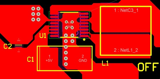
另外我的layout是如图的 有什么问题没有?
是的,如果负载电阻太大,芯片会启动不了。。
芯片启动不了是指没有输出,还是说输出不到5V? 谢谢你的回答。
PCB layout看起来还好
你现在能不能做个实验,将负载变为电子负载,使用恒流模式,启动的时候空载,等输出电压变为5V后,然后逐渐增加负载电流,使负载电流增加至1A,看看这种情况下输出能否保持5V
做完实验请回复一下
When the device enables the internal start-up cycle starts with the first step, the precharge phase. During precharge, the rectifying switch is turned on until the output capacitor is charged to a value close to the input voltage. The rectifying switch current is limited in that phase. This also limits the output current under short-circuit conditions at the output. After charging the output capacitor to the input voltage the device starts switching. Until the output voltage is reached, the boost switch current limit is set to 40% of its nominal value to avoid high peak currents at the battery during startup. When the output voltage is reached, the regulator takes control and the switch current limit is set back to 100%.
想确认下是否是这个原因引起的
确实是因为这个问题,开始电阻太小,电流被限死,导致电压被拉低。 现在已经明白,我从10欧开始减少电阻,当电阻减小到3欧左右,已经能输出1.5A以上电流,并且电压不降低。 谢谢你的回答,另外请问下,为什么这个芯片设定为这样,是不得已为之还是为了别的原因?
因为输入源是电池,inrush current会对电池造成损伤,所以要控制inrush current
在使用的时候TPS61032的负载一般都有enable功能,可以通过LBO延时启动负载,这样可以有效减小inrush current
不好意思,后半句我没理解。什么叫通过LBO延时启动负载? LBO是指什么呢?
LBO是低电压输入指示信号
这个了解,我是想问如何通过LBO来延时启动负载?
Roy wu1
确实是因为这个问题,开始电阻太小,电流被限死,导致电压被拉低。 现在已经明白,我从10欧开始减少电阻,当电阻减小到3欧左右,已经能输出1.5A以上电流,并且电压不降低。 谢谢你的回答,另外请问下,为什么这个芯片设定为这样,是不得已为之还是为了别的原因?
这颗芯片支持大输出电容,在VOUT上升到VIN之前用近似恒流充输出电容可以防止过度从电池抽电,另外还可以起到短路保护作用。
目前比较新的boost控制器多有这一功能。