UCC28070 加入直流偏置至电流检测信号中的目的?
看了UCC28070的应用手册,对这个还是不理解,看上面的图,感觉加了直流直流偏置至电流检测信号中那这就不是真实的电感电流了?手册上的语句我可能还没明白,这个问题阻碍了我的设计,工作人员能否帮我翻译一下,谢谢!
To improve noise immunity at extremely light loads, a PWM ramp with a dc offset is recommended to be added to the current sense signals. Electrical components RTA, RTB, CTA, CTB, DPA1, DPA2, DPB1, and DPB2 form a PWM ramp that is activated and deactivated by the gate drive outputs of the UCC28070. Resistor ROA and ROB add a DC offset to the CS resistors (RSA and RSB).
When the inductor current becomes discontinuous the boost inductors ring with the parasitic capacitances in the boost stages. This inductor current rings through the CTs causing a false current sense signal.Refer to the following graphical representation of what the current sense signal looks like when the
inductor current goes discontinuous. Note that the inductor current and VRSA may vary from this graphical representation depending on how much inductor ringing is in the design when the unit goes discontinuous.
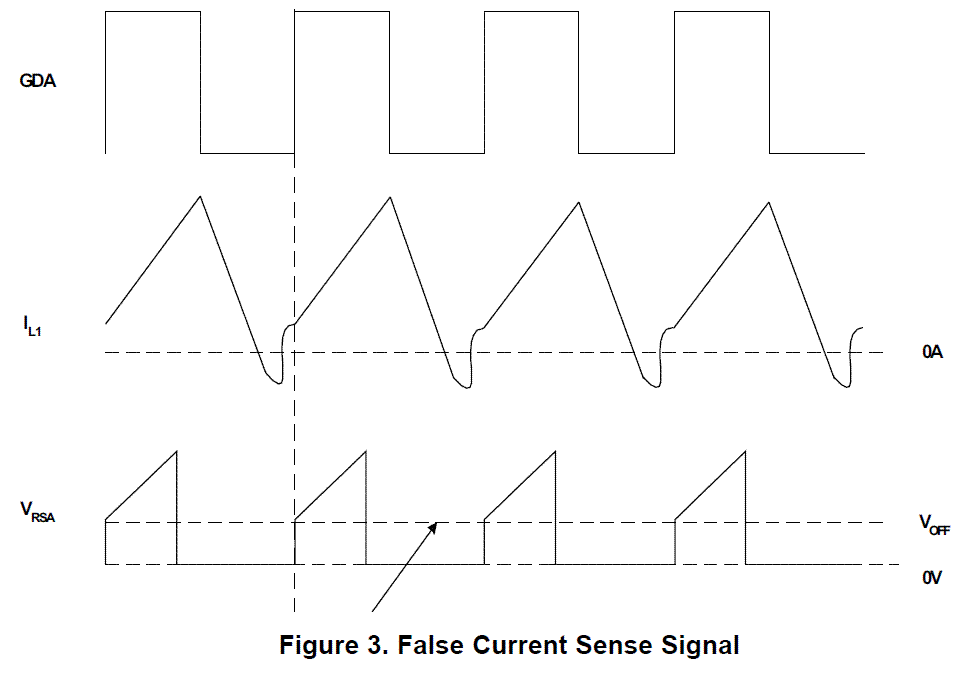
To properly select the offset (VOFF) just requires adjusting resistors ROA and ROB to add a dc offset to the current sense resistors, that is high enough to block DRA and DRB from conducting when a false current sense signals is present. This occurs when the inductors are operating with discontinuous inductor current and was described above in detail. Setting the offset to 200 mV is a good starting point and may need to be adjusted based on individual design criteria and the amount of noise and parasitic elements present in the system.
自已顶!
而且,加入直流偏置后,Vrsa也应该是到不了0的,应该是不会低于Voff的呀!
没看到具体电路图,猜测的
1、加入补偿后,可以提高抗干扰能力,地线上一般会有一些噪声,我们假设100mV,当轻载的时候,如果取样信号下雨100mV,那么有用信号就会被噪声淹没,电路就可能失效。而增加补偿后,如果加入200mV,那么即使轻载的时候,采样信号也会比200mV高,就可以提高抗干扰能力勒。
2、加入的直流偏置,从示意图上看,只是在由驱动信号的时候才有补偿,当驱动信号消失,补偿也自动消失,那么在没有驱动信号的时候,采样仍然为0。
不知道是否可以解答你的疑惑?