HDC2010 底部PCB Layout
时间:10-02
整理:3721RD
点击:
HDC2010 的传感元件位于器件底部,请问下,这种PCB Layout在HDC2010底部是怎么处理?是打一个大孔?还是做焊盘接地?
看看官方手册的参考
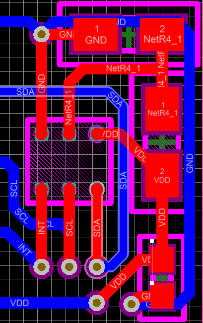
请参考datasheet 有关10.1 layout guideline部分的介绍:http://www.ti.com/lit/ds/symlink/hdc2010.pdf
It is recommended to isolate the sensor from the rest of the PCB by eliminating copper layers below the device (GND, VDD) and creating a slot into the PCB around the sensor to enhance thermal isolation.