opa695电流负反馈运算放大器
While this design may still yield acceptable results in the application, it is a simple matter to adjust these
resistor values slightly to get perfect gain match from the two output currents to the amplifier output and
also provide exactly the same apparent resistive load to each output. Implementing this adjustment also
moves in the direction of giving better channel linearity and, therefore, lower distortion. Achieving matched
gain magnitudes also moves the mid-scale DC output (when both output currents are equal to IP/ 2)
closer to 0V at the op amp output. The designs here assumed bipolar supplies for the op amp where a 0V
output is desired when each DAC channel is at (I
P
/ 2) (midscale). While there might be other, more
dominant, distortion mechanisms that mask this improvement, it is preferable to remove this unmatched
output voltage swing as a possible source of imbalance.
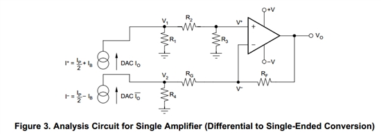
To balance this design, start with the full design circuit of Figure 3, and write the gain and input impedance
equations looking into each port. Define the desired gain as G (which will be an impedance) and input
impedance Ζ
i
(which will also be an impedance).这是opa695datesheet的一段话,对应图,谁能告诉我
 输入端的ip.iB分别指什么啊?
楼主你好!
能否上传下你提到的文档或者文档号,opa695 datasheet没有查到你贴出来的这段。
您好,是在opa696的应用手册里有
Wideband Complementary Current Output DAC to
Single-Ended Interface: Improved Matching
for the Gain and Compliance Voltage Swing第三页的图里有
我的另一个问题是这个文档的仿真结果是用tian90软件分析的吗?在TIAN9里面没有找到dB欧姆(在第7页的图的纵坐标)。还有此文中分别给了同向增益和反向增益公式。我想用opa695做增益为1的差动转单端的功能,那这两个增益有什么作用,他们要怎么匹配?