LMC660输出震荡
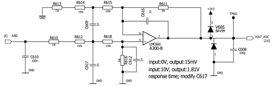
(1). Schematics: from below , you can see situation of application, AIB2 is input analog voltage :0-10V, VOLT_ADC is output voltage :0-1.81V.
(2). Different batch IC
|
Description 2 |
Name |
Part number |
Quantity |
Manufacturing date |
Status |
|
70CPE02358 |
NATIONAL SEMICONDUCTOR |
LMC660AIMX/NOPB |
2500 |
2013/1/4 |
Stock: 2384 |
|
70CPE02358 |
NATIONAL SEMICONDUCTOR |
LMC660AIMX/NOPB |
1550 |
2010/10/18 |
Used up |
|
70CPE02358 |
NATIONAL SEMICONDUCTOR |
LMC660AIMX/NOPB |
550 |
2010/12/30 |
Used up |
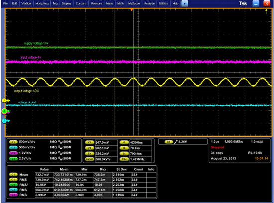
We used the batch(2010/10/18 and 2010/12/30), when input voltage(AIB2) is 4Vdc, the voltage output(VOLT_ADC) after Amp is stable(yellow is amp output). It is good!

When supplier changed to new batch(2013/1/4) which is used for the first time, when input voltage(AIB2) is also 4Vdc, the voltage output(VOLT_ADC) after amp is not stable(yellow), output voltage occurred oscillation ! Freq=1.4MHz, AM=160mV.
Why using the same IC which batch is only different, the output voltage occurred oscillation? Please give us some support about this issue as soon as possible! Thanks!
Mr Shi,
您这个电路设计的不够完善,不稳定应该是由于容性负载导致。
批次不同,导致的结果不同,原因:
1,由于这个电路的相位裕度设计的不够足,所以,电路处于震荡的临界位置,换了新批次的货,可能工作就震荡了。
2,另外,进货渠道有没有问题,是不是正规渠道。
参考附件中的电路,在电容反馈回路和电阻反馈回路中间加一个隔离电阻,类似附件图中的做法。
Best Regards,
Iven Xu
hi lven,
谢谢你的回复!我会按照你的方法进行改进的!如何提高相位裕度设计?请赐教!谢谢
7411.运放驱动容性负载 (1).doc