提高PA效率来增加手机的通话时间
System designers must be very cautious and do a power survey of every component on the phone’s pcb. The RF power amplifier (PA) powered directly from the battery sticks out like a sore thumb from the power budget perspective.
Cellular and WLAN standards have been evolving with data transmission speeds that started from 14.4 kbits/s in CDMA-1 to 2 Mbits/s in CDMA2000/WCDMA. Modulation schemes used in CDMA and WCDMA result in a modulated signal that exhibits a non-constant amplitude envelope.
The need to utilize the available spectrum efficiently and transmit at high data rates necessitates the use of modulation schemes that use both amplitude and phase changes to encode information. Consequently, PAs must operate with linear gain and phase relationships from input-to-output; these linear PAs inherently operate at lower efficiency as compared to saturated PAs in older/slower transmit schemes such as GSM. This efficiency decrease is primarily due to the quiescent operating point being backed off from the PA’s compression point.
The amount of back-off is determined by the complementary cumulative distribution function (CCDF) of the transmitted signal which in turn depends on the wireless standard and the number of active RF channels being transmitted by the handset. When the handset is operating in transmit mode, the RF power section consumes up to 65% of the overall power budget as a result of the PAs intrinsic inefficiencies.
RF PAs used in WCDMA cellular standards have been traditionally powered directly from the battery. This maintains the linearity of the RF PA at the expense of PA (and system) efficiency.
The requirement for linear PAs in systems that have both amplitude- and phase-modulation components require system designers to balance linearity and efficiency requirements in new handset designs. The use of dc-to-dc switching converters to supply the optimal voltage to the RF PA brings about a 50% to 200% improvement in average PA efficiency based on typical RF power transmit probability distributions for WCDMA systems. This improvement has been observed for commercial RF PAs with different architectures such as those with either switched gain stages or conventional Class A/AB multi-stage designs.
For this reason, linear PAs powered by magnetic buck converters can dramatically increase system efficiency. Overall efficiency (OE) or power-added efficiency (PAE) of the PA is a key performance metric of a power amplifier.
OE = RF_Pout /(Pdc+RF_Pin)
The key in using a switcher unit for a PA (SUPA) is to reduce the Pdc factor in the denominator for a given RF_Pout and RF_Pin while maintaining linearity (ACPR/ACLR specs). The supply voltage can be changed with an SUPA to a level that will ensure that the PA’s gain doesn’t decrease significantly and the amplifier operates in a linear manner in response to the input signal and doesn’t compress the output signal.
A quantitative measurement of linearity for a modulated signal is the adjacent-channel-power/leakage ratio. PA gain is typically specified under specific channel and RF_Pout conditions. The change in gain with respect to the amplifier’s supply voltage is specific to the PA manufacturer; while PA manufacturers generally don’t provide these curves in their datasheet, designers can characterize this or request the data.
When the PA is connected directly to the battery, Pdc = Vbatt×Ibatt and when it’s powered by a SUPA, Pdc = Vo×Io. It can be seen that by increasing the PA’s overall efficiency, all that’s needed is a low Vo compared to Vbatt. This is achieved by lowering the SUPA’s output voltage at lower transmitted RF power levels. This in turn reduces Io (the current drawn by the PA) and results in a lower input current drawn from the battery due to the dc-to-dc converter’s inherent high efficiency. Note that behaviorally, PAs can be modeled as RF_Pin and Vcc_PA controlled resistors.
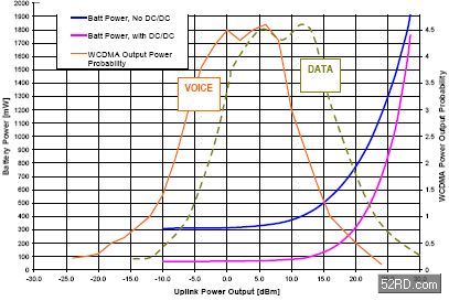
It’s important to consider the power probability profile of transmit power to understand the impact of savings in powering a PA with a SUPA (Fig. 1). The Tx power probability is dependent on the wireless standard and carrier system design/usage. The profiles are different for urban and rural regions.
|
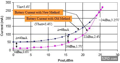
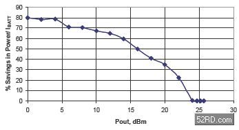
The dc-to-dc converter’s output voltage must be varied as the transmitted power levels are changed to maintain the ACPR specs (Fig. 2). The savings in battery current can be as high as 50 mA in the 0- to 20-dBm power levels. The PA is most often operating in this band of power levels.
|
|
A good question to ask is why we have to change the dc-to-dc converter voltage as the transmitted power level is increased. The answer is that this is needed to maintain the ACPR ratios. Adjacent channel power/leakage ratio helps characterizes the PA’s distortion and other subsystems for their tendency to cause interference with neighboring radio channels or systems. It’s specified as the ratio of the power spectral density (PSD) of the main channel to the PSD measured at several offset frequencies. Violating the ACLR specs will lower the voice quality, as well as decrease wireless system capacity.
If the supply voltage to the PA is not increased as Pout is increased, the ACLR specifications can’t be met. The 3GPP system-level spec for WCDMA is -34 dBc, and to preserve sufficient margin caused by temperature and device variances, the ACLR value of -38 dBc is used for PA measurements.
The key requirements of buck converters for powering RF PAs are:
- High efficiency over wide output voltage and load ranges. The LM3208 has an efficiency of 96% at Vin = 4.2 V, Vo = 3.4 V, Io = 400 mA (high RF power), and 87% at Vin = 3.9 V, Vo = 1.5 V, Io = 100 mA (low RF power). It also employs dynamic RDSon management to further improve the efficiency at low output voltages by automatically reducing the FET sizes to minimize switching losses. Low output voltages are associated with low RF output power, which translates to low output currents for the SUPA. Switching losses dominate at light loads for a switcher and the key advantage of using smaller FETs are smaller gate capacitances and lower gate charge losses.
- Dynamic output voltage adjustment. The LM3208 output voltage can be adjusted form 0.8 to 3.6 V using an external voltage. The gain from this input to Vo is 2.5.
- 30-μs output slew rate and settling. In a WCDMA architecture, transmit power is adjusted by ±1 dB in every 667 μs as requested by the basestation. There’s a 50-μs window at the beginning of every 667-μs transmit cycle in which the Vcon adjustments must be completed. The LM3208 meets this spec.
- Well-behaved drop-out. The Low RDSon PFET (140 mΩ) and bypass FET (LM3204) gives low dropout voltage. Pulse skipping gives low ripple near 100% duty cycle.
- Low duty cycle operation for low output voltages. A minimum on time of 50 ns in the LM3208 facilitates a 10% duty-cycle operation for output voltages of 0.8 V and lower depending on the Vin range.
- High switching frequency. The LM3208’s 2-MHz switching frequency allows for the use of smaller sized external components and meeting spectral emission requirements.
- Fast turn-on time. The LM3208 has a 40-μs turn-on time for Vo = 3.4 V from EN = low to high. This meets the time mask requirements for transmit on/off.
Buck converters for powering RF PAs are specialized in their function and are different when compared to a buck converter powering a digital core processor.
Areas where there are considerable differences are in the features. For example, quiescent current (Iq) is a critical spec for a buck converter powering a digital core processor as the processor spends a lot of time in varius standby modes (100 μA typical, drawn from the buck converter). In the case of an RF PA, even at no output power, the PA consumes around 50 mA which negates the need for ultra low quiescent current specs. A SUPA buck has an Iq of 700 μA (typical) compared to 16 μA, (typical) for a digital core buck, such as the LM3671.
In a second example, transient response for a buck converter powering a digital core processor is optimized for load transients and line transients. Output current requirements are expected to change depending on the processor’s state. In the case of a SUPA, the key transient parameter is the Vcon transient, changing the output voltage from a low value to a higher value or vice versa without undershoots or overshoots and within the target time.
Finally, in a third example, switching FET sizes for a buck converter are optimized based on the operation’s duty cycle. For a digital core processor, the typical duty cycle varies from 30% to 60%. For a SUPA, the duty cycle can vary from 10% to 100%. Low dropout voltage requirements also dominate the FET RDSon values for a SUPA.
Application circuits
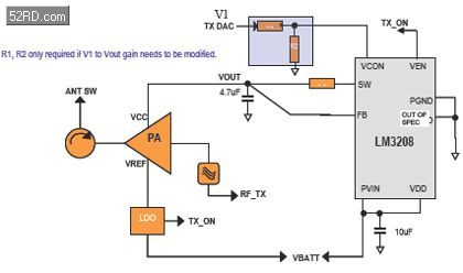
In a design where the baseband directly controls Vo, the analog baseband chip contains a DAC (Fig. 3). The PA is characterized and uses a lookup table scheme of PA_supply voltage vs. PA_RFout. Because the baseband has the information of the required RF output power into the antenna (commanded by the basestation), it commands the DAC to put out the required Vcon voltage.
|
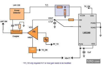
When a power detector is used to set Vo, the power detector is part of a closed loop and sets the output voltage (Fig. 4). This is known as the envelope following technique described that utilizes the RF signal envelope information as the feedback signal to set the PA’s supply voltage. There’s no in-band distortion products associated with amplitude nonlinearity.
Harmonic distortion products are generally not an issue and can be removed with simple filtering if it becomes a problem. In this scheme, the RF output signal is sampled by a directional coupler and fed into a peak power detector, such as the LMV228. The LMV228’s output power detector is a dc signal that’s proportional to the RF input power’s envelope magnitude. This dc signal forms the SUPA’s Vcon signal. The PA supply voltage (SUPA output voltage) is thus controlled by the PA’s RF power output.
|
Looking at some data comparing battery life with and without SUPA (LM3208), consider the WCDMA PA section by itself. To calculate total run times, other blocks in the handset must be considered. The PA is being operated as per the WCDMA probability distribution curve.
Two scenarios are considered: the PA operated continuously in high power mode, and the PA operated in low and high power modes (bias switching PA), depending on the output power transmitted (see the table).
|
The input voltage is 3.4 V and the run times are computed using the average battery power. A bigger improvement can be expected at higher supply voltages considering the Li-Ion battery’s voltage range. Note the use of smaller capacity battery for the run-time calculations with SUPA. This implies that smaller capacity batteries can be used for cost savings and/or reducing the form factor of mobile handsets.
About the author
Mathew Jacob is an applications engineering manager at National Semiconductor Corp. He holds a Bachelors degree in Electronics and Communication Engineering from Madurai Kamaraj University in India. Jacob can be reached at Mathew.Jacob@nsc.com.
Jay Rajagopalan, Jeff Huard, and Frank De Stasi contributed to this article.

