有哪位高手知道什么是IC的Strap Pin?
strapping pin: 我的理解是通过外部跳线连接决定输入电平,达到选择内部多功能选择的目的。这类pin往往有丰富的复用功能,比如在上电复位期间选择某种功能,但正常工作时又定义为其他用法。
strapping pin 可能就是复用管脚,如有的phy芯片支持自动识别线序功能,用这种芯片做出的网络接口,可以和别的网口采用直通线相连也可以用交叉线相连,其发送和接收线是复用的,就叫strapping pin。
通过一个pin 电平的高低来控制另外一些pin的输出选择
这个被控制的pin就叫strip pin
应该是这样...
二楼正解
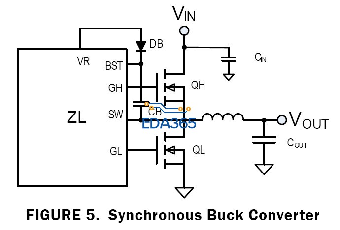
Intersil Synchronous Buck Datasheet
Typically, buck converters specify a maximum duty cycle that effectively limits the maximum output voltage that can be realized for a given input voltage. This duty cycle limit ensures that the lowside MOSFET is allowed to turn on for a minimum amount of time during each switching cycle, which enables the bootstrap capacitor (CB in Figure 5) to be charged up and provide adequate gate drive voltage for the high-side MOSFET. See section “High-side Driver Boost Circuit” on page 12 for more details.
High-side Driver Boost Circuit
The gate drive voltage for the high-side MOSFET driver is generated by a floating bootstrap capacitor, CB (see Figure 5). When the lower MOSFET (QL) is turned on, the SW node is pulled to ground and the capacitor is charged from the internal VR bias regulator through diode DB. When QL turns off and the upper MOSFET (QH) turns on, the SW node is pulled up to VDD and the voltage on the bootstrap capacitor is boosted approximately 5V above VDD to provide the necessary voltage to power the high-side driver. A Schottky diode should be used for DB to help maximize the high-side drive supply voltage.
最近看数据手册也有碰到这个名词,受教了~