千兆网(PHY芯片)数据丢包
自动协商模式
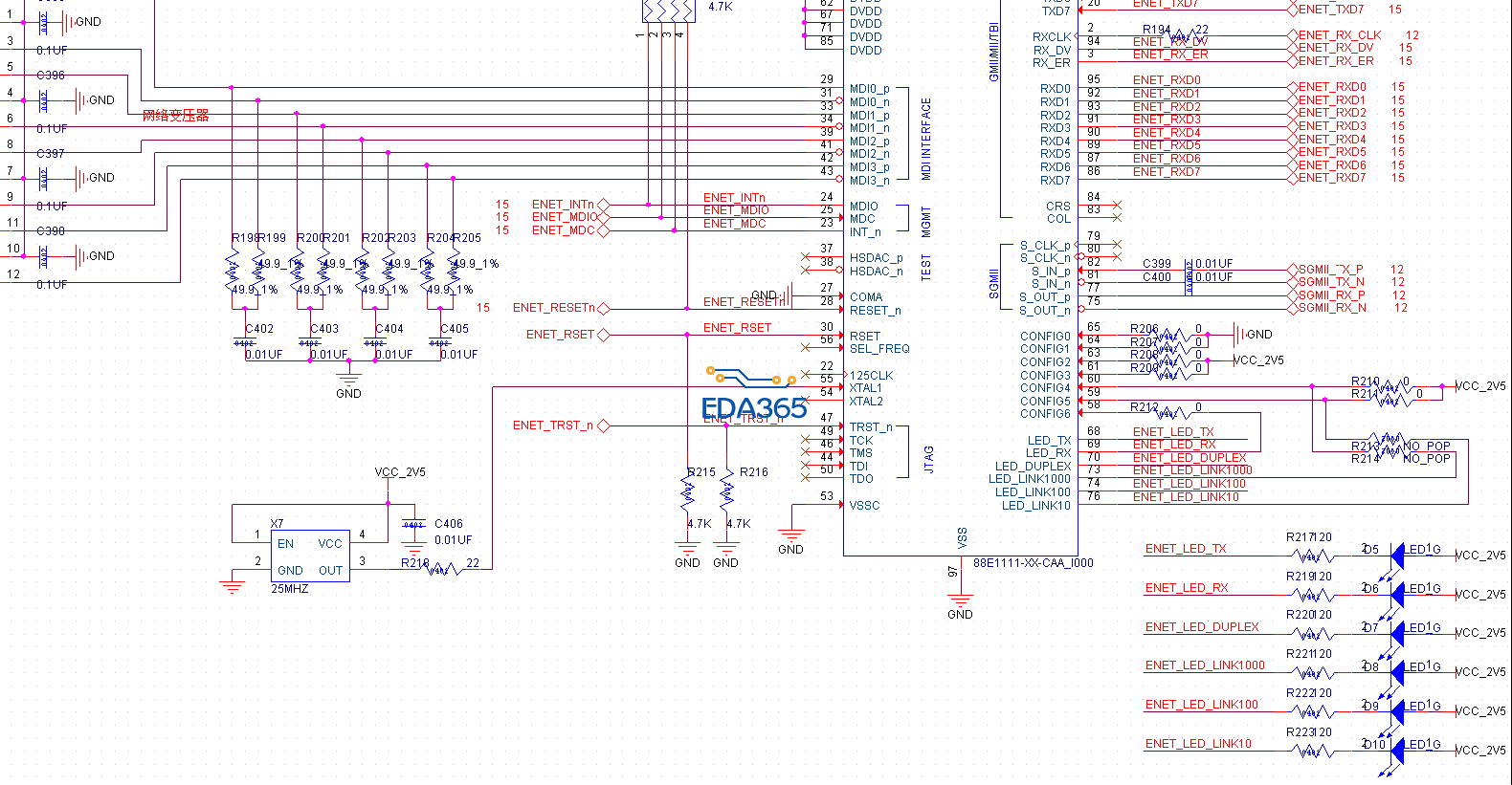
GMII模式
终端电阻50ohm
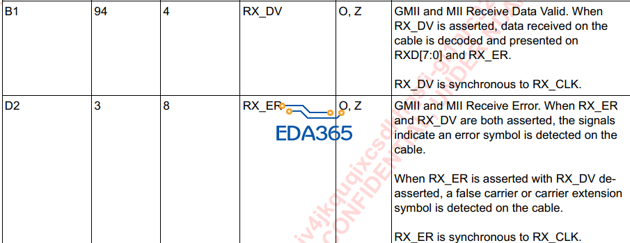
a false carrier or carrier extension symbol is detected on the cable.
具体指的什么?
求指教,有没有人知道啊~~~
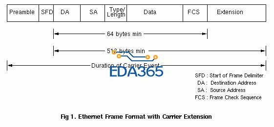
Carrier Extension
Gigabit Ethernet should be inter-operable with existing 802.3 networks. Carrier Extension is a way of maintaining 802.3 minimum and maximum frame sizes with meaningful cabling distances. For carrier extended frames, the non-data extension symbols are included in the "collision window", that is, the entire extended frame is considered for collision and dropped. However, the Frame Check Sequence (FCS) is calculated only on the original (without extension symbols) frame. The extension symbols are removed before the FCS is checked by the receiver. So the LLC (Logical Link Control) layer is not even aware of the carrier extension. Fig. 1 shows the ethernet frame format when Carrier Extension is used.
你可以看一下那個問 "1000M RJ45 差分线等长要求" 的貼文嗎?
Intel Design Guide 最後一句話說,走線不對稱或不等長會影響接收資料的正確率。
先確認 PCB Layout 是否有做好?
还是小编热心!
PCB Layout应该没有问题,几块样板中50%正常;也一直怀疑线路的问题,做了多种测试也没定位到具体位置。
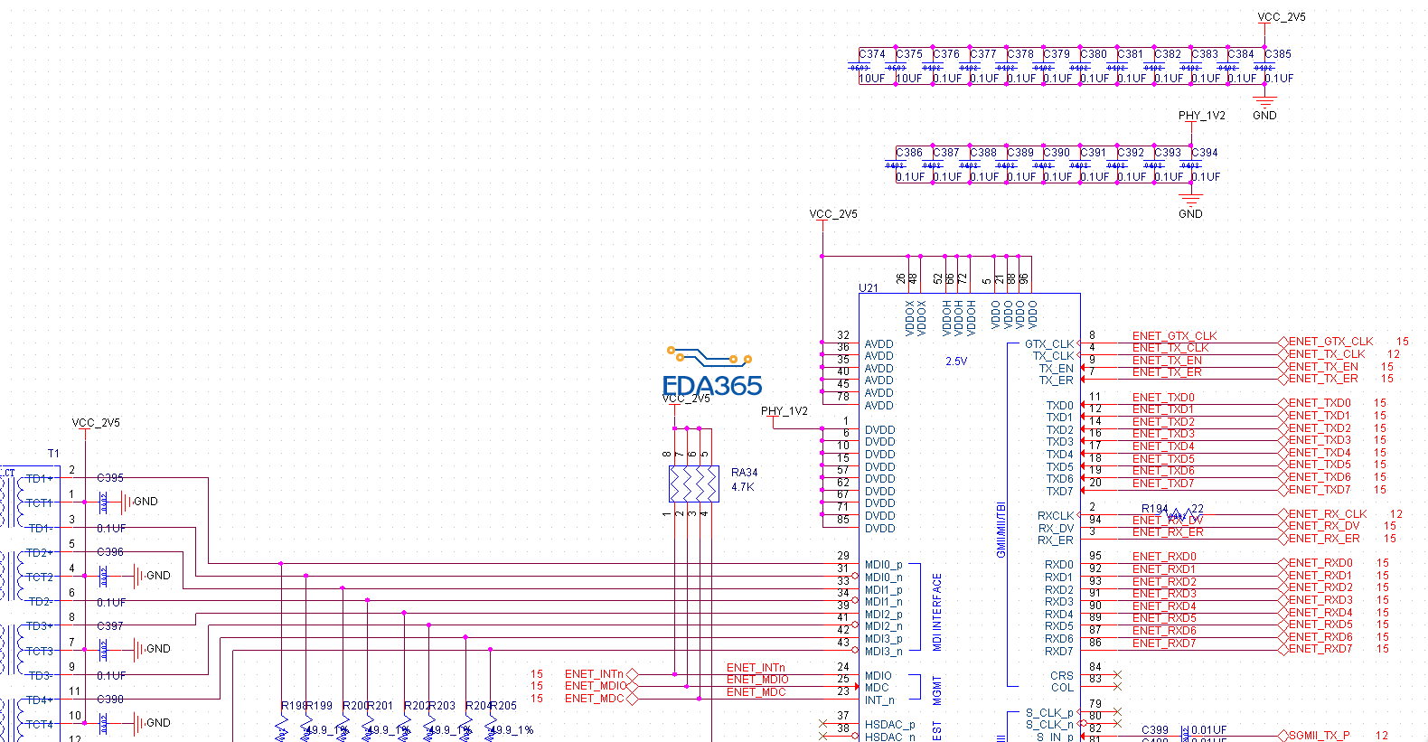
好像TX和RX要在发射端串33ohm的端接电阻,这个会影响丢包与否。还有就是晶振的ppm值过大有频偏的话也会影响丢包,要换更高精度的晶体。
CPU与交换芯片的通讯GRMII总线要串33ohm的端接电阻!
33欧姆电阻要靠近TX放置,估计和时钟有很大关系,你看看marvell的PHY芯片对OSC晶振的供电有无要求?
这个原理图只是丢包?能工作?
23、24、25管脚连对了?
这个地方是网络标号名称标错了
R218短路现象一样,电源 AVDD目前板子上不好隔离,一样的电路在其他板卡(与PHY连接的FPGA型号不一样)上没有出现丢包的现象
由于空间有限,33ohm串阻没有加,tx使用的是FPGA片内的串阻,RX端就没有,晶振测试更换过现象依旧。这个交换芯片在其他板卡上(cpu不同)没有出现该现象,问题应该是线路上不稳定,几块板卡丢包的程度不一样。
兄弟,最后问题怎么解的?